Boron Arsenide
https://www.youtube.com/watch?v=YNHyLeTCP3s
Cubic Boron Arsenide: The Future of Super-Semiconductors! // LaVand MEDIA.
Discover the incredible potential of cubic boron arsenide (BAs) in our latest video! Learn how this powerful combination of boron and arsenic forms a robust crystal with unique properties. Explore ongoing research efforts aimed at unlocking BAs's revolutionary potential. As a fantastic conductor of heat and an efficient semiconductor, BAs holds promise for creating faster, more powerful computer chips and improving thermal management in devices like phones, computers, and electric vehicles. Understand the challenges scientists face in developing defect-free BAs crystals and how overcoming these obstacles could shape the future of technology. Don't miss out on this exciting journey into the future of electronics and thermal management!
https://www.youtube.com/watch?v=j0GWe3btZoI
Rice researchers set record for quantum vibrations in boron arsenide // Smalley-Curl Institute | Rice University
Rice researchers, led by Hanyu Zhu, have demonstrated record-long quantum vibrations in boron arsenide, where optical phonons can persist nearly 10 times longer than in typical materials. Published in Physical Review Letters, the study highlights a new pathway for controlling heat and information at the quantum level.
https://www.youtube.com/watch?v=5nsa0y83kqg
Breakthrough in Boron Arsenide Crystals // ScienceHubNet
A recent study published in the journal Materials Today highlights an exciting advancement in our understanding of heat conduction in solids. Boron arsenide crystals have been produced with exceptional purity, allowing them to achieve thermal conductivity values exceeding two thousand one hundred watts per meter per Kelvin at room temperature. This surpasses diamond, long considered the gold standard for heat conduction.
Professor Zhifeng Ren from the University of Houston, a co-author of the study, expressed confidence in the precision of their measurements. He suggests that these surprising results might require scientists to rethink and adjust current theoretical models to align with this new experimental data.
This breakthrough is the result of a fruitful collaboration between the Texas Center for Superconductivity at the University of Houston, the University of California Santa Barbara, and Boston College. For over a decade, boron arsenide has intrigued researchers with its theoretical potential to conduct heat as well as or even better than diamond. However, earlier models had underestimated its capabilities due to complex factors like phonon scattering, leading many to doubt its potential.
Ren's team believed the key issue lay in the impurities within the material rather than its inherent ability. By refining the arsenide and improving manufacturing techniques, they created boron arsenide crystals with significantly fewer defects. This high purity allowed the material to demonstrate an astonishing thermal conductivity that not only exceeded previous experimental results but also surpassed theoretical predictions.
This discovery underscores the critical role of material purity in heat transfer performance, opening doors to the development of more efficient thermal conductors. Beyond the lab, boron arsenide's implications are vast. It offers a promising alternative for semiconductors in devices requiring advanced thermal management, such as smartphones, high-power electronics, and data centers.
Boron arsenide's benefits extend beyond its impressive heat conduction. It's easier and cheaper to produce than diamond and doesn't require extreme temperatures or pressures. It also boasts excellent semiconductor properties, potentially outperforming silicon due to its high carrier mobility, wide bandgap, and thermal expansion compatibility.
This discovery marks a new chapter in our understanding of heat conduction in solid materials, highlighting the importance of revisiting current theoretical models. Researchers are keen to continue enhancing boron arsenide's performance, potentially unlocking new frontiers in thermal materials and semiconductors. This work demonstrates the importance of pushing beyond existing theories to uncover new possibilities that can reshape our scientific understanding.
https://www.youtube.com/shorts/jBWUEql4EgI
Heat travels in rays inside this crystal.
Wikipedia.org
Boron arsenide
Chemical formula BAs
Molar mass 85.733 g/mol[1]
Appearance Brown cubic crystals[1]
Density 5.22 g/cm3[1]
Melting point 1,100 °C (2,010 °F; 1,370 K) decomposes[1]
Solubility in water Insoluble
Band gap 1.82 eV
Thermal conductivity 1300 W/(m·K) (300 K)
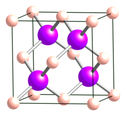
Crystal structure Cubic (sphalerite), cF8, No. 216
Space group F43m
Lattice constant a = 0.4777 nm
Formula units (Z)4
CAS Number 12005-70-8
Properties
Chemical formula B12As2
Molar mass 279.58 g/mol
Density 3.56 g/cm3[3]
Solubility in water Insoluble
Band gap 3.47 eV
Structure[4]
Crystal structure Rhombohedral, hR42, No. 166
Space group R3m
Lattice constant a = 0.6149 nm, b = 0.6149 nm, c = 1.1914 nm , α = 90°, β = 90°, γ = 120°
Formula units (Z)6
Boron arsenide (or Arsenic boride) is a chemical compound involving boron and arsenic, usually with a chemical formula BAs. Other boron arsenide compounds are known, such as the subarsenide B12As2. Chemical synthesis of cubic BAs is very challenging and its single crystal forms usually have defects.
Properties
BAs is a cubic (sphalerite) semiconductor in the III-V family with a lattice constant of 0.4777 nm and an indirect band gap of 1.82 eV. Cubic BAs is reported to decompose to the subarsenide B12As2 at temperatures above 920 °C.[5] Boron arsenide has a melting point of 2076 °C. The thermal conductivity of BAs is exceptionally high, measured in single-crystal BAs to be around 1300 W/(m·K) at room temperature, making it the highest among all metals and semiconductors.
The basic physical properties of cubic BAs have been experimentally measured:[7] Band gap (1.82 eV), optical refractive index (3.29 at wavelength 657 nm), elastic modulus (326 GPa), shear modulus, Poisson's ratio, thermal expansion coefficient (3.85×10⁻⁶/K), and heat capacity.
It can be alloyed with gallium arsenide to produce ternary and with indium gallium arsenide to form quaternary semiconductors
BAs has high electron and hole mobility, >1000 cm2/V/second, unlike silicon which has high electron mobility, but low hole mobility.
In 2023, a study in journal Nature reported that subjected to high pressure BAs decreases its thermal conductivity contrary to the typical increase seen in most materials.
Boron subarsenide
Boron arsenide also occurs as subarsenides, including the icosahedral boride B12As2. It belongs to R3m space group with a rhombohedral structure based on clusters of boron atoms and two-atom As–As chains. It is a wide-bandgap semiconductor (3.47 eV) with the extraordinary ability to "self-heal" radiation damage.[13] This form can be grown on substrates such as silicon carbide.[14] Another use for solar cell fabrication[8][15] was proposed, but it is not currently used for this purpose.
Applications
Boron arsenide is most attractive for use in electronics thermal management. Experimental integration with gallium nitride transistors to form GaN-BAs heterostructures has been demonstrated and shows better performance than the best GaN HEMT devices on silicon carbide or diamond substrates. Manufacturing BAs composites was developed as highly conducting and flexible thermal interfaces.
First-principles calculations have predicted that the thermal conductivity of cubic BAs is remarkably high, over 2,200 W/(m·K) at room temperature, which is comparable to that of diamond and graphite.[17] Subsequent measurements yielded a value of only 190 W/(m·K) due to the high density of defects. More recent first-principles calculations incorporating four-phonon scattering predict a thermal conductivity of 1400 W/(m·K).[20] Later, defect-free boron arsenide crystals have been experimentally realized and measured with an ultrahigh thermal conductivity of 1300 W/(m·K), consistent with theory predictions. Crystals with small density of defects have shown thermal conductivity of 900–1000 W/(m·K).
The cubic-shaped boron arsenide has been discovered to be better at conducting heat and electricity than silicon, as well as reportedly better than silicon at conducting both electrons and its positively charged counterpart, the "electron-hole."
https://www.science.org/doi/10.1126/science.aat7932
Unusual high thermal conductivity in boron arsenide bulk crystals
Fei T, et al.
Moving the heat aside with BAs
Thermal management becomes increasingly important as we decrease device size and increase computing power. Engineering materials with high thermal conductivity, such as boron arsenide (BAs), is hard because it is essential to avoid defects and impurities during synthesis, which would stop heat flow. Three different research groups have synthesized BAs with a thermal conductivity around 1000 watts per meter-kelvin: Kang et al., Li et al., and Tian et al. succeeded in synthesizing high-purity BAs with conductivities half that of diamond but more than double that of conventional metals (see the Perspective by Dames). The advance validates the search for high-thermal-conductivity materials and provides a new material that may be more easily integrated into semiconducting devices.
Abstract -- Conventional theory predicts that ultrahigh lattice thermal conductivity can only occur in crystals composed of strongly bonded light elements, and that it is limited by anharmonic three-phonon processes. We report experimental evidence that departs from these long-held criteria. We measured a local room-temperature thermal conductivity exceeding 1000 watts per meter-kelvin and an average bulk value reaching 900 watts per meter-kelvin in bulk boron arsenide (BAs) crystals, where boron and arsenic are light and heavy elements, respectively. The high values are consistent with a proposal for phonon-band engineering and can only be explained by higher-order phonon processes. These findings yield insight into the physics of heat conduction in solids and show BAs to be the only known semiconductor with ultrahigh thermal conductivity.
https://www.science.org/doi/10.1126/science.aat8982
High thermal conductivity in cubic boron arsenide crystals
Sheng Li et al
https://journals.aps.org/prl/abstract/10.1103/PhysRevLett.121.105901
Antisite Pairs Suppress the Thermal Conductivity of BAs
Qiang Zheng et al
Abstract -- BAs was predicted to have an unusually high thermal conductivity with a room temperature value of 2000 W m−1 K−1
, comparable to that of diamond. However, the experimentally measured thermal conductivity of BAs single crystals is still lower than this value. To identify the origin of this large inconsistency, we investigate the lattice structure and potential defects in BAs single crystals at the atomic scale using aberration-corrected scanning transmission electron microscopy (STEM). Rather than finding a large concentration of As vacancies (ݑAs ), as widely thought to dominate the thermal resistance in BAs, our STEM results show an enhanced intensity of some B columns and a reduced intensity of some As columns, suggesting the presence of antisite defects with AsB (As atom on a B site) and BAs (B atom on an As site). Additional calculations show that the antisite pair with AsB next to BAs is preferred energetically among the different types of point defects investigated and confirm that such defects lower the thermal conductivity for BAs. Using a concentration of 1.8(8)% (6.6±3.0×1020 cm−3 in density) for the antisite pairs estimated from STEM images, the thermal conductivity is estimated to be 65–100 W m−1 K−1 , in reasonable agreement with our measured value. Our study suggests that AsB−BAs antisite pairs are the primary lattice defects suppressing thermal conductivity of BAs. possible approaches are proposed for the growth of high-quality crystals or films with high thermal conductivity. Employing a combination of state-of-the-art synthesis, STEM characterization, theory, and physical insight, this work models a path toward identifying and understanding defect-limited material functionality.
https://phys.org/news/2013-07-competitor-diamond-thermal-conductor.html
An unlikely competitor for diamond as the best thermal conductor
by Boston College
...The high thermal conductivity of diamond is well understood, resulting from the lightness of the constituent carbon atoms and the stiff chemical bonds between them, according to co-author David Broido, a professor of physics at Boston College. On the other hand, boron arsenide was not expected to be a particularly good thermal conductor and in fact had been estimated – using conventional evaluation criteria – to have a thermal conductivity 10 times smaller than diamond.
The team found the calculated thermal conductivity of cubic boron arsenide is remarkably high, more than 2000 Watts per meter per Kelvin at room temperature and exceeding that of diamond at higher temperatures, according to Broido and co-authors Tom Reinecke, senior scientist at the Naval Research Laboratory, and Lucas Lindsay, a post-doctoral researcher at NRL who earned his doctorate at BC.
Broido said the team used a recently developed theoretical approach for calculating thermal conductivities, which they had previously tested with many other well-studied materials. Confident in their theoretical approach, the team took a closer look at boron arsenide, whose thermal conductivity has never been measured.
Unlike metals, where electrons carry heat, diamond and boron arsenide are electrical insulators. For them, heat is carried by vibrational waves of the constituent atoms, and the collision of these waves with each other creates an intrinsic resistance to heat flow. The team was surprised to find an unusual interplay of certain vibrational properties in boron arsenide that lie outside of the guidelines commonly used to estimate the thermal conductivity of electrical insulators. It turns out the expected collisions between vibrational waves are far less likely to occur in a certain range of frequencies. Thus, at these frequencies, large amounts heat can be conducted in boron arsenide.
https://arxiv.org/abs/1911.11281
Basic Physical Properties of Cubic Boron Arsenide
Joon Sang Kang, Man Li, Huan Wu, Huuduy Nguyen, Yongjie Hu
[ PDF ]
Abstract -- Cubic boron arsenide (BAs) is an emerging semiconductor material with a record-high thermal conductivity of 1300 W/mK. However, many fundamental properties of BAs remain unexplored experimentally. Here, for the first time, we report the systematic experimental measurements of important physical properties of BAs, including the bandgap, optical refractive index, stiffness, elastic modulus, shear modulus, Poisson ratio, thermal expansion coefficient, and heat capacity. In particular, light absorption and Fabry Perot interference were used to measure an optical bandgap of 1.82 eV and a refractive index of 3.29 (657 nm) at room temperature. A pico-ultrasonic method, based on ultrafast optical pump probe spectroscopy, was used to measure a high elastic modulus of 326 GPa, which is twice that of silicon. Furthermore, temperature dependent X-ray diffraction was used to measure a linear thermal expansion coefficient of 3.85x10^-6 per K; this value is very close to prototype semiconductors such as GaN, which underscores the promise of BAs for cooling high power and high frequency electronics. We also performed ab initio theory calculations and observed good agreement between the experimental and theoretical results. Importantly, this work aims to build a database (Table I) for the basic physical properties of BAs with the expectation that this semiconductor will inspire broad research and applications in electronics, photonics, and mechanics.
https://palmstrom.cnsi.ucsb.edu/research/boron-arsenide-growth
Boron Arsenide Growth
Boron arsenide (BAs) is an exceptional semiconductor material with remarkable properties and significant technological potential. With an ultra-high thermal conductivity of approximately 1300 W/m·K and a similar lattice structure to other semiconductors, BAs excels at heat dissipation. This makes it invaluable for thermal management in high-power electronics and integrated circuits. High intrinsic electron and hole mobilities (electron: 1,400 cm2/Vs, hole: 2,110 cm2/Vs), positions it as an ideal candidate for next generation semiconductor devices. In our research, we seek to successfully synthesize thin films of BAs for the first time utilizing molecular beam epitaxy. We are currently utilizing both elemental and chemical forms of boron and arsenic to attempt to achieve this goal.
https://www.nature.com/articles/s41467-025-60038-3
Nature Communications volume 16, Article number: 4755 (2025)
Synthesis of hexagonal boron arsenide nanosheets for low-power consumption flexible memristors
Zenghui Wu, et al
[ PDF ]
Abstract -- Boron arsenide has recently attracted significant attention for its thermal and electronic properties. However, its lengthy growth process and bulk structure limit its application in advanced semiconductor systems. In this study, we introduce a method for synthesizing ultrathin crystalline hexagonal boron arsenide (h-BAs) nanosheets in large quantities via an in-situ chemical reaction of sodium borohydride with elemental arsenic in a low-pressure hydrogen atmosphere. We successfully fabricated h-BAs-based memory devices with ON/OFF current ratios up to 109, low energy consumption of less than 4.65 pJ, and commendable stability. Furthermore, we have developed flexible h-BAs-based memristors with good stability and robustness. This research not only provides a promising avenue for synthesizing h-BAs nanosheets, but also underscores their potential in the development of next-generation electronic devices.
https://journals.aps.org/prl/abstract/10.1103/qysd-d6rn
Phys. Rev. Lett. 136, 116903 – Published 20 March, 2026
DOI: https://doi.org/10.1103/qysd-d6rn
Exceptional Optical Phonon Coherence in Enriched Cubic Boron Arsenide via Suppression of Three-Phonon Scattering
Tong Lin, et al.
Abstract -- Cubic boron arsenide (BAs) is a promising semiconductor for next-generation electronics due to its outstanding ambipolar mobility and thermal conductivity, the latter of which is attributed to the suppression of three-phonon scattering. However, precisely accounting for different high-order anharmonic scattering processes is challenging from both theory and experiment, so that questions remain open regarding the ultimate limit of phonon lifetime and thermal conductivity in BAs. Here we show that this gap nearly eliminates three-phonon scattering for zone-center optical phonons in a wide temperature range, leading to a record-high, isotope purity-limited phonon coherence with a quality factor above 3.7×10³
for >98% enriched 11BAs below 100 K. We discriminate three decoherence mechanisms by their temperature-dependent contribution to the damping rate using high-resolution Raman and Fourier transform infrared spectroscopy. For the as-synthesized crystals, we find that defect scattering has negligible contributions to the linewidth of optical phonons in comparison to isotope scattering. These results provide critical insights into the intrinsic and extrinsic scattering mechanisms of optical phonons in BAs, motivating further studies to quantify anharmonic effects and realize superior phonon transport.
https://phys.org/news/2026-03-boron-arsenide-semiconductor-quantum-vibrations.html
Boron arsenide semiconductor sets record in quantum vibrations
https://advanced.onlinelibrary.wiley.com/doi/10.1002/advs.202502544
Isotope-Enriched Cubic Boron Arsenide with Ultrahigh Thermal Conductivity
Jaehoon Kim, Dongwook Lee, Huan W
Abstract -- High thermal conductivity materials are critical for advanced thermal management applications. The semiconductor cubic boron arsenide (c-BAs) has drawn significant attention due to its ultrahigh thermal conductivity. In this study, high-quality isotope-enriched cubic boron arsenide (c-10BAs and c-11BAs) crystals are synthesized to further enhance the thermal conductivity of c-BAs and measured a room temperature thermal conductivity of 1500 W m−1 K−1 for the c-11BAs. This value is the highest thermal conductivity for isotope-enriched c-BAs reported so far. The experimental study, together with ab initio calculation, verifies the high quality with reproducibility of the crystals. The exceptionally high thermal conductivity of the isotope-enriched BAs, combined with their semiconductor properties, holds significant potential for improving thermal management in semiconductor devices and electronics packaging applications.
1 Introduction
Thermal management is an essential technology for a wide range of electronic devices, including power electronics and optoelectronics. A common approach to achieving efficient thermal management involves utilizing materials with high thermal conductivity to effectively spread heat from localized hot spots. A material with thermal conductivity higher than that of copper (400 W m−1 K−1) is considered to be a high thermal conductivity material, but there is limited choice of materials that exceed that value. Diamond has the highest thermal conductivity (2200 W m−1 K−1) among known bulk materials. However, high synthesis cost, chemical inertness, and slow growth rate hinder the practical application of diamond. On the other hand, graphite suffers from highly anisotropic thermal conductivity because of the weak van der Waals bonding between each layer, resulting in low cross-plane thermal conductivity. Therefore, for efficient thermal management, an alternative high-thermal conductivity material is necessary.
Cubic boron arsenide (c-BAs) has attracted significant interest due to its ultrahigh thermal conductivity. First-principles calculations estimate the thermal conductivity of BAs to be ≈2000 W m−1 K−1, assuming only three-phonon scattering—the lowest order phonon-phonon interaction. However, when four-phonon scattering is included, the calculated thermal conductivity decreases to a range of 1300–1400 W m−1 K−1. These theoretical predictions have been experimentally confirmed, establishing BAs as one of the highest thermal conductivity materials among known semiconductors.
In addition, c-BAs exhibits high ambipolar carrier mobility, distinguishing it from other high-thermal conductivity materials. Theoretically, c-BAs possesses exceptionally high hole mobility (2100 cm2 V−1 s−1), surpassing that of silicon (450 cm2 V−1 s−1) and common III-V semiconductor materials such as GaN (40 cm2 V−1 s−1) and GaAs (400 cm2 V−1 s−1). High ambipolar mobility of 1600 cm2 V−1 s−1 was experimentally confirmed, highlighting its potential for p-type semiconductor applications Furthermore, this material demonstrates lower thermal boundary resistance with typical semiconductors and metals due to its phonon band structure. For instance, a GaN-on-BAs structure exhibits a thermal boundary conductance (TBC) of 250 MW m⁻2 K⁻¹, significantly higher than that of a GaN-on-diamond structure. The combination of high thermal conductivity, mobility, and superior TBC makes c-BAs a promising candidate for efficient heat dissipation in advanced electronic devices.
Previous studies have focused on enriching boron isotopes to further enhance the thermal conductivity of c-BAs.[16, 17] Despite these efforts, experimental measurements have recorded only minimal differences in thermal conductivity between isotope-enriched and natural c-BAs (c-natBAs). Most experimental results report thermal conductivity values in the range of 1100–1300 W m−1 K−1, regardless of isotopic composition. Given that isotope-enriched crystalline solids typically exhibit higher thermal conductivity compared to their natural counterparts,[18, 19] these previous results suggest that impurities may have a more pronounced influence than isotope composition in the c-BAs samples. Furthermore, significant variations in thermal conductivity have been observed among c-BAs crystals synthesized using identical crystal growth methods,[20, 21] even within the same batch. Local defects within individual crystals have also led to considerable deviations in measured thermal conductivity,[12] complicating precise comparisons between natural and isotope-enriched c-BAs.
We recently reported a highly reproducible c-BAs synthesis using a transitional metal as a catalyst.[22] Here, in this study, we expand our synthesis technique to isotope-enriched c-BAs (c-10BAs and c-11BAs) to further increase the thermal conductivity of c-BAs. The impurity concentrations of the synthesized c-10BAs and c-11BAs samples were characterized using Raman spectroscopy and compared to previous studies, and the free-charge carrier concentration in our samples remained at exceptionally low levels. By using time-domain thermoreflectance (TDTR) measurements, we systematically measured the thermal conductivity of c-10BAs and c-11BAs as well as c-natBAs. The maximum thermal conductivity of the isotope-enriched BAs reached ∼1500 W m−1 K−1, surpassing the previously reported experimental values of 1300 W m−1 K−1. Additionally, ab initio calculations were employed to theoretically study the thermal conductivity of isotope-enriched c-BAs with c-natBAs. A comparison between the experimental data and theoretical calculation revealed that the experimentally measured values exceeded those calculated by ab initio models. These findings highlight the potential of isotope-enrichment strategies, combined with optimized synthesis techniques, to achieve superior thermal properties in c-BAs, thereby advancing its applicability for high-performance thermal management.
2 Results and Discussion
We synthesized high-quality c-natBAs, c-10BAs, and c-11BAs using a modified chemical vapor deposition method. Cubic BAs has a zinc blende crystal structure in an F4 3ݑ space group with a primitive cell containing two atoms. The lattice structure of synthesized c-BAs with respect to different boron isotopes is shown in Figure 1a. The structure features tetrahedral bonding, where each boron atom is covalently bonded to four arsenic atoms, and each arsenic atom to four boron atoms. Since arsenic exists as a single isotope element, the isotope effect that affects thermal conductivity in c-BAs is solely determined by boron. Naturally occurring boron (natB) consists of two stable isotopes, 19% of 10B, and 81% of 11B. This results in an average atomic mass of 10.81 for the natB. Figure 1b shows optical images of three different c-BAs isotope crystals. The majority of the crystals exhibit a semi-transparent reddish hue, with dimensions ranging from a few hundred micrometers (100 to 400 µm) and a consistent morphology, predominantly hexagonal or semi-hexagonal.
2 Results and Discussion
We synthesized high-quality c-natBAs, c-10BAs, and c-11BAs using a modified chemical vapor deposition method. Cubic BAs has a zinc blende crystal structure in an F4
3ݑ space group with a primitive cell containing two atoms. The lattice structure of synthesized c-BAs with respect to different boron isotopes is shown in Figure 1a. The structure features tetrahedral bonding, where each boron atom is covalently bonded to four arsenic atoms, and each arsenic atom to four boron atoms. Since arsenic exists as a single isotope element, the isotope effect that affects thermal conductivity in c-BAs is solely determined by boron. Naturally occurring boron (natB) consists of two stable isotopes, 19% of 10B, and 81% of 11B. This results in an average atomic mass of 10.81 for the natB. Figure 1b shows optical images of three different c-BAs isotope crystals. The majority of the crystals exhibit a semi-transparent reddish hue, with dimensions ranging from a few hundred micrometers (100 to 400 µm) and a consistent morphology, predominantly hexagonal or semi-hexagonal.
https://pubs.aip.org/aip/apl/article/124/22/222201/3295458/Highly-reproducible-synthesis-of-boron-arsenide
Highly reproducible synthesis of boron arsenide with high thermal conductivity
Dongwook Lee, Jaehoon Kim, Joon Sang Kang
Cubic boron arsenide (BAs) is a subject of considerable interest in thermal science due to its exceptionally high thermal conductivity. However, the inherent long mean free path of phonons renders the thermal conductivity of BAs highly susceptible to impurity concentration. In this study, we present a catalyst assisted crystal synthesis approach to achieve high-quality cubic BAs, leveraging Pt as a catalyst in the synthesis process. Our thermal conductivity measurements reveal that over 90% of the samples in a batch exhibit thermal conductivity values exceeding 1000 W·m−1·K−1. The robustness of the synthesis method is further validated through thermal conductivity mapping and Raman spectroscopy. These findings offer valuable insights for enhancing the quality of BAs crystals and hold promise for practical applications.
https://journals.aps.org/prb/abstract/10.1103/PhysRevB.96.161201
Four-phonon scattering significantly reduces intrinsic thermal conductivity of solids
Tianli Feng1, Lucas Lindsay2, and Xiulin Ruan1
Abstract -- For decades, the three-phonon scattering process has been considered to govern thermal transport in solids, while the role of higher-order four-phonon scattering has been persistently unclear and so ignored. However, recent quantitative calculations of three-phonon scattering have often shown a significant overestimation of thermal conductivity as compared to experimental values. In this Rapid Communication we show that four-phonon scattering is generally important in solids and can remedy such discrepancies. For silicon and diamond, the predicted thermal conductivity is reduced by 30% at 1000 K after including four-phonon scattering, bringing predictions in excellent agreement with measurements. For the projected ultrahigh-thermal conductivity material, zinc-blende BAs, a competitor of diamond as a heat sink material, four-phonon scattering is found to be strikingly strong as three-phonon processes have an extremely limited phase space for scattering. The four-phonon scattering reduces the predicted thermal conductivity from 2200 to 1400 W/m K at room temperature. The reduction at 1000 K is 60%. We also find that optical phonon scattering rates are largely affected, being important in applications such as phonon bottlenecks in equilibrating electronic excitations. Recognizing that four-phonon scattering is expensive to calculate, in the end we provide some guidelines on how to quickly assess the significance of four-phonon scattering, based on energy surface anharmonicity and the scattering phase space. Our work clears the decades-long fundamental question of the significance of higher-order scattering, and points out ways to improve thermoelectrics, thermal barrier coatings, nuclear materials, and radiative heat transfer.
Boron Arsenide Patents
Boron arsenide indirect-direct band gap transformation method based on deep strain regulation and application
CN121653852
The invention discloses a boron arsenide indirect-direct band gap transformation method based on deep strain regulation and application, the boron arsenide indirect-direct band gap transformation method based on deep strain regulation is characterized by comprising the following steps: S1, applying uniaxial tensile strain to a boron arsenide crystal; s2, directional transformation of boron arsenide from an indirect band gap to a direct band gap is achieved by controlling the strain direction, the strain range and the relaxation condition after strain loading, the uniaxial tensile strain is applied in the [111] crystal orientation of boron arsenide crystals, the tensile strain is controlled within the elastic limit range, and the tensile strain is applied in the [111] crystal orientation of the boron arsenide crystals; the band gap type transformation is completed when the tensile strain reaches the critical transformation strain, indirect-direct band gap transformation can be completed only by applying 0.12 tensile strain in the [111] direction, the transformation condition is clear and controllable, and the photoelectron transition efficiency is greatly improved.
Cosolvent forboron arsenide growth crystal, cubic boron arsenide crystal and synthesis method of cubic boron arsenide crystal
CN121183399
The invention discloses a cosolvent for a boron arsenide growth crystal, a cubic boron arsenide crystal and a synthesis method of the cubic boron arsenide crystal, and relates to the technical field of boron arsenide crystal synthesis. The synthesis method comprises the following steps: placing a container in which boron and the cosolvent are sealed in a vacuum manner in double-temperature-zone heating equipment, heating a high-temperature end to 800-920 DEG C, heating a low-temperature end to 650-850 DEG C, enabling the high-temperature end to be at least 20 DEG C higher than the low-temperature end, cooling the high-temperature end from a crystallization initial temperature to a crystallization final temperature at a rate of 10 DEG C/h or below after heat preservation treatment, and cooling the high-temperature end to a crystallization final temperature at a rate of 10 DEG C/h or below; the cubic boron arsenide crystal is obtained. The antimony-arsenic alloy melt is adopted as a cosolvent to dissolve boron, the temperature distribution of the melt is controlled by controlling the temperature of the high-temperature end and the low-temperature end, meanwhile, slow cooling is conducted at the high-temperature end at a low speed, low-pressure liquid phase growth of cubic boron arsenide is achieved, and the synthesis method improves the crystal quality and size, reduces the system pressure and improves the yield of cubic boron arsenide. And the method has lower requirements on equipment and is suitable for industrial mass production.
Method for calculating and regulating boron arsenide band gap based on first principle
CN120998370
The invention discloses a method for calculating and regulating a boron arsenide band gap based on a first principle, and the method comprises the steps: applying uniaxial stretching or compression depth strain to boron arsenide in the Z-axis direction and diagonal direction of a cubic unit cell and the equal-height symmetrical direction of the diagonal direction of the cubic unit cell body; vASP and vaspkit software are combined for modeling, static calculation, energy band calculation and band gap extraction, and precise regulation and control of the band gap are achieved. According to the method, the change rule of the band gap under strain in different directions is defined, the theoretical calculation process is simple and efficient, experimental design and sample preparation can be effectively guided, the experimental efficiency is greatly improved, the time and material cost is reduced, and an important theoretical basis is provided for diversified application of boron arsenide in the field of semiconductor devices.
High-thermal-conductivity boron arsenide ceramic substrate and preparation method and application thereof
CN120565503
The invention discloses a high-thermal-conductivity boron arsenide ceramic substrate and a preparation method and application thereof, and relates to the technical field of microelectronic materials. According to the high-thermal-conductivity boron arsenide ceramic substrate provided by the invention, the buffer layer of which the thermal expansion coefficient is within a specific range is introduced between the boron arsenide substrate and the conductive layer for transition, and the thickness of the buffer layer is controlled according to the difference of the thermal expansion coefficients of materials on two sides of the buffer layer, so that the stress between layers in the ceramic substrate can be reduced, and the thermal conductivity of the ceramic substrate is improved. And the long-acting stability of the substrate is improved while the excellent heat-conducting property is considered.
Production process of boron arsenide film crystal
CN120273026
The invention discloses a production process of a boron arsenide film crystal, and belongs to the technical field of compound semiconductor material synthesis. The process comprises the following steps: step 1, placing a silicon substrate in a deposition chamber, and starting a molecular pump to vacuumize the deposition chamber; 2, argon is used as carrier gas, and borane is carried into the deposition chamber; then argon is used as carrier gas, and arsine is carried into the deposition chamber; 3, heating the deposition chamber, preserving heat after heating is completed, then electrifying to continuously release a high-voltage arc, forming arsenic and boron in an ionic state under bombardment of the high-voltage arc, and growing a cubic boron arsenide thin film wafer on the silicon substrate; and 4, after the reaction is completed, cooling to room temperature, and taking out a product to obtain a finished product of the epitaxial cubic boron arsenide thin film wafer on silicon. The plasma technology is adopted, argon is used for carrying arsine and borane, the cubic boron arsenide thin film wafer grows on the silicon substrate, and the method has the advantages of being lower in reaction temperature, higher in reaction efficiency, good in safety and the like.
SEMICONDUCTOR STRUCTURE INCLUDING HIGH THERMAL CONDUCTIVITY MATERIAL AND METHOD OF FORMING THE SAME
US2025254902
Provided are a semiconductor structure including high kappa (high-K) material for source/drain (S/D) and/or thermal heat spreader and a method of forming the same. The semiconductor device includes a substrate, a plurality of channel layers stacked over the substrate, a gate structure wrapping the plurality of channel layers, and source/drain (S/D) regions disposed over the substrate at opposite sides of the gate structure and connecting the plurality of channel layers. A material of the S/D regions includes a high thermal conductivity material with a single crystal structure, such as boron arsenide (BAs) with a thermal conductivity greater than 1000 W/mK. In this case, the high thermal conductivity material can efficiently dissipate the heat generated by the semiconductor structure to enhance the yield and the reliability of the semiconductor structure.
METHODS FOR HIGH QUALITY BORON ARSENIDE SINGLE CRYSTAL GROWTH
WO2025072815
Methods for producing a single crystal boron arsenide, and single crystal boron arsenide produced by the methods are disclosed. In one aspect, the method includes contacting elemental boron with elemental arsenic to form a reaction mixture; maintaining the reaction mixture at a temperature above melting point of arsenic for an effective amount of time to form a product mixture comprising the single crystal boron arsenide and liquid arsenic; cooling the product mixture for a predetermined amount of time; and separating the liquid arsenic from the single crystal boron arsenide.
BORON ARSENIDE OF HIGH THERMAL CONDUCTIVITY AND SYNTHESIS METHOD THEREOF
KR102783297
The present invention relates to non-boron monocrystal and a method for manufacturing the same. A method for manufacturing arsenic boron comprises the steps of: preparing high purity boron powder, arsenic powder, and flux crystal powder; mixing the boron powder, the arsenic powder, and the flux crystal powder; sealing the boron powder, the arsenic powder, and the flux crystal powder in a vacuum state in a reactor; controlling the temperature of the reactor and synthesizing arsenic boron; and lowering the temperature of the reactor and separating the flux crystal from the synthesized arsenic boron.
Preparation method of boron arsenide film
CN119194595
The invention discloses a preparation method of a boron arsenide film, which comprises the following steps: growing a cubic phase boron arsenide film material on the surface of a two-dimensional Van der Waals material (single layer or multiple layers) in a Van der Waals epitaxy mode, so that nucleation sites are uniform and controllable, and boron arsenide can uniformly form a film on the two-dimensional Van der Waals material; compared with the preparation of boron arsenide single crystals, the preparation method provided by the invention can effectively overcome the technical obstacles that the growth thickness and uniformity of the boron arsenide thin film, the crystal quality, the performance stability and the like are difficult to control; the prepared boron arsenide film is suitable for preparation and application of semiconductor electronic materials.
Equipment for preparing gallium arsenide single crystal and preparation method of gallium arsenide single crystal
CN118979307
The invention discloses equipment for preparing a gallium arsenide single crystal and a preparation method of the gallium arsenide single crystal, and belongs to the technical field of semiconductors. By adopting the equipment, the preparation of the gallium arsenide single crystal with high crystal forming rate and low dislocation density defect can be realized. According to the preparation method of the gallium arsenide single crystal, the stability of a temperature field in a furnace is controlled through a magnetic field generated by a magnet in the single crystal growth furnace, so that the thermal stability of a gallium arsenide polycrystal melt is ensured, and the quality of the gallium arsenide single crystal is remarkably improved. Moreover, according to the preparation method, boron oxide does not need to be additionally added, boron oxide is obtained through direct reaction of oxygen and a boron nitride crucible, the boron oxide is sealed, and then stable air pressure in the stepped quartz tube is maintained through nitrogen, so that the chemical proportion balance of gallium arsenide is maintained. In addition, according to the preparation method, metal impurity ions are reduced through hydrogen, metal impurity elementary substance segregation is promoted through ultrasonic vibration, holes, agglomeration and stress aggregation are reduced, the dislocation density defect is further reduced, and the crystallization rate of the gallium arsenide single crystal is increased.
DEVICE FOR PRODUCING AN ACOUSTIC WAVE, AND RADIO FREQUENCY FILTER AND MULTIPLEXER COMPRISING THE SAME
WO2024170071
The present disclosure relates to a cubic Boron Arsenide, c-BAs, based multi-layered device configured to produce an acoustic wave. The device comprises a c-BAs-based substrate (102), a piezoelectric layer (104) provided on the c-BAs-based substrate, and an Interdigital Transduce, IDT (108, 110), provided on the piezoelectric layer. The IDT is configured to excite the acoustic wave in response to an applied RF signal. The device further comprises a temperature compensation, TC, layer (106) either provided between the c-BAs-based substrate and the piezoelectric layer or covering the piezoelectric layer and the IDT. By using the c-BAs-based substrate, it is possible to minimize the number of propagating spurious acoustic waves at different material interfaces in the device. Thus, the suppression of the spurious acoustic wave modes is provided without having to use any external components (e.g., combinations of capacitors, inductors, transformers, etc.) or additional resonators in a RF circuit in which the device is to be used.
STRUCTURE COMPRISING A HIGH THERMAL CONDUCTIVITY BORON ARSENIDE LAYER, AND METHOD OF MANUFACTURE
US20260209990
A structure for microelectronic applications, extending along an extension plane, includes a crystalline boron arsenide BAs layer having two dimensions, each of at least 2 cm, respectively along two directions normal to each other and included in the extension plane.
Ultra-high ambipolar mobility cubic boron arsenide
US2023257907
Herein provided are cubic boron arsenide (c-BAs) single crystals having an unexpectedly high ambipolar mobility at room temperature, µ<a>, at one or more locations thereof that is greater than or equal to 1500, 1600, 1700, 1800, 1900, 2000, 2100, 2200, 2300, 2400, 2500, 2600, 3000, 4000, 5000, 6000, 7000, 8000, 9000, or 10000 cm<2>V<-1>s<-1>, wherein the ambipolar mobility is defined as: µ<a> = 2µ<e>µ<h>/(µ<e> + µ<h>), wherein µ<e> is electron mobility and µ<h> is hole mobility, and having a room temperature thermal conductivity at the one or more locations thereof that is greater than or equal to 1000 Wm<-1>K<-1>. Methods of making and using the c-BAs single crystals are also provided.
Boron arsenide resonant tunneling diode and manufacturing method thereof
CN116314350
The invention discloses a boron arsenide resonant tunneling diode which mainly solves the problems that an existing gallium nitride resonant tunneling diode is asymmetric in energy band structure, has no bidirectional symmetric differential negative resistance characteristic and is low in peak current and peak-valley current ratio. The device comprises a substrate, an epitaxial layer, an emitter ohmic contact layer, a first isolation layer, a first barrier layer, a quantum well layer, a second barrier layer, a second isolation layer, a collector ohmic contact layer and a collector. And an annular emitter is arranged on the emitter ohmic contact layer. Wherein the first barrier layer and the second barrier layer are made of boron arsenide materials with the same thickness, the emitter and collector ohmic contact regions are made of n-type boron gallium indium arsenic materials with the same components and thicknesses, the first isolation layer, the second isolation layer and the quantum well layer are made of boron gallium indium arsenic materials with the same components, and the substrate is made of boron arsenide single crystals with high thermal conductivity. The device has no spontaneous polarization effect and bidirectional symmetrical differential negative resistance effect, has a high ratio of peak current to peak-valley current, and can be used for a terahertz wave source and a digital logic circuit.
Heat dissipation structure and power module assembly
CN115666100
he invention provides a heat dissipation structure and a power module assembly. The heat dissipation structure comprises a first heat conductor and a second heat conductor. The first heat conductor comprises a body, an input port and an output port, wherein the input port and the output port protrude out of the body. The body is provided with a first groove and a second groove which are oppositely arranged. The first groove communicates with the input port and the output port, the input port is used for inflow of cooling liquid, and the output port is used for outflow of the cooling liquid. And a first fin group is arranged in the second groove. The second heat conductor comprises a heat conduction substrate and a second fin set connected with the heat conduction substrate, the second fin set is contained in the first groove, and the material of the second heat conductor comprises boron arsenide. According to the heat dissipation structure and the power module assembly, by arranging the first heat conductor and the second heat conductor which have the liquid cooling effect and the air cooling effect, an air cooling and liquid cooling multi-medium heat dissipation channel is constructed, and therefore the heat dissipation effect can be greatly improved.
Boron arsenide nanocrystal synthesized by mechanochemical method as well as preparation method and application of boron arsenide nanocrystal
CN115321552
The invention provides a heat dissipation structure and a power module assembly. The heat dissipation structure comprises a first heat conductor and a second heat conductor. The first heat conductor comprises a body, an input port and an output port, wherein the input port and the output port protrude out of the body. The body is provided with a first groove and a second groove which are oppositely arranged. The first groove communicates with the input port and the output port, the input port is used for inflow of cooling liquid, and the output port is used for outflow of the cooling liquid. And a first fin group is arranged in the second groove. The second heat conductor comprises a heat conduction substrate and a second fin set connected with the heat conduction substrate, the second fin set is contained in the first groove, and the material of the second heat conductor comprises boron arsenide. According to the heat dissipation structure and the power module assembly, by arranging the first heat conductor and the second heat conductor which have the liquid cooling effect and the air cooling effect, an air cooling and liquid cooling multi-medium heat dissipation channel is constructed, and therefore the heat dissipation effect can be greatly improved.
Boron arsenide nanocrystal prepared from oxide as well as preparation method and application of boron arsenide nanocrystal
CN115259174
The invention discloses a boron arsenide nanocrystal prepared from oxide as well as a preparation method and application of the boron arsenide nanocrystal. The preparation method comprises the following steps: mixing arsenic trioxide, boron oxide powder and magnesium particles according to a ratio in air, filling the mixture into a ball milling tank, carrying out a mechanochemical reaction for a certain time, removing impurities in the mixed powder, and carrying out wet grinding purification and acid treatment to obtain boron arsenide (such as B12As2) nanocrystal powder. The method is simple and convenient to operate, arsenic trioxide can be converted into boron arsenide which is stable in chemical property and high in thermal stability, and the method has potential application prospects in the fields of nuclear radiation protection, isotope radiation batteries and related photoelectric materials. Meanwhile, the technology can be popularized and applied to harmless and stable treatment of arsenic trioxide-containing waste residues or smoke dust.
Preparation method of boron arsenide powder
CN115196645
The invention discloses a preparation method of boron arsenide powder, and relates to the field of preparation of boron arsenide powder. The method comprises the following steps: cleaning a crucible, carrying out ultrasonic treatment on the crucible, and drying for later use; uniformly mixing alkaline earth metal EA, boron arsenate and a molten salt medium, and putting the mixture into a crucible; the method comprises the following steps: reducing boron arsenate BAsO4 according to a reaction formula BAsO4 + 4EA = BAs + 4EA (O), putting a crucible into a reaction furnace, introducing argon protective gas, heating to 700-900 DEG C, and keeping the temperature for 1-5 hours; and 3, soaking the sample obtained in the step 2 in concentrated hydrochloric acid at room temperature, heating in a water bath, preserving heat, washing with deionized water to be neutral, and carrying out ball milling and drying to obtain the boron arsenide powder. According to the method, high-pressure or complex equipment is not needed, boron arsenide can be provided in a simple and economical mode within a short time, and the defects of methods in the prior art are overcome; the method can be used for preparing a boron arsenide target material and preparing a boron arsenide single crystal thin film material by a physical vapor phase method; and the difficulty of preparing the boron arsenide single crystal material is reduced.
Surface acoustic wave resonator, manufacturing method thereof and filter
CN115208348
The embodiment of the invention discloses a surface acoustic wave resonator, a manufacturing method thereof and a filter. The surface acoustic wave resonator includes: a substrate; the high sound velocity layer is located on the substrate, and the material of the high sound velocity layer comprises boron arsenide; and the piezoelectric layer is positioned on one side, far away from the substrate, of the high-sound-velocity layer. According to the technical scheme, the power bearing capacity of the filter can be enhanced, and the frequency and performance of the filter are improved.
FLEXIBLE THERMAL INTERFACE BASED ON SELF-ASSEMBLED BORON ARSENIDE FOR HIGH-PERFORMANCE THERMAL MANAGEMENT
US2024055320
A thermal interface comprising a polymer composite comprising a polymer and a self-assembled boron arsenide.
Double-temperature-zone dense tube synthesis technology of boron arsenide powder material
CN114105157
The invention relates to the technical field of double-temperature-zone dense-tube synthesis of boron arsenide powder materials, and discloses a double-temperature-zone dense-tube synthesis technology of boron arsenide powder materials, which specifically comprises the following steps: accurately weighing boron powder with the purity of 99.999% and arsenic particles with the purity of 99.999%, then loading the weighed boron powder and arsenic particles into quartz tubes, with the loading amount of each tube being 50-100g, the molar ratio of boron to arsenic being 1: (1.5-1.9), the length of the quartz tubes being 750-1100mm, and the loading amount of the quartz tubes being 1: (1.5-1.9); a high-temperature end and a low-temperature end are arranged at two ends of the tube, boron is arranged at the high-temperature end, and arsenic is arranged at the low-temperature end; vacuumizing the quartz tube until the air pressure in the quartz tube is 0.01 torr, and sealing the quartz tube; a quartz tube is heated in a double-tube synthesis furnace, the high-temperature end is heated to 800-890 DEG C, the low-temperature end is heated to 500-615 DEG C, heat preservation is conducted for 2-6 days, a product is purified and then subjected to ball milling, and cubic boron arsenide powder with the purity being 99.995 or above is obtained and can be used for preparing a high-purity boron arsenide target material or a cubic boron arsenide single crystal material.
Unusual high thermal conductivity in boron arsenide bulk crystals
US2021269318
A method for growing bulk boron arsenide (BA) crystals, the method comprising utilizing a seeded chemical vapor transport (CVT) growth mechanism to produce single BAs crystals which are used for further CVT growth, wherein a sparsity of nucleation centers is controlled during the further CVT growth. Also disclosed are bulk BAs crystals produced via the method.
Vertical cavity surface emitting laser and manufacturing method thereof
CN110137801
The invention discloses a vertical cavity surface emitting laser and a manufacturing method thereof, and belongs to the technical field of semiconductors. The vertical cavity surface emitting laser comprises a substrate, a heat dissipation layer, a lower reflection layer, a light emitting region, an upper reflection layer, an upper metal electrode and a lower metal electrode. The heat dissipationlayer, the lower reflection layer, the light emitting region, the upper reflection layer and the upper metal electrode are sequentially stacked on the first surface of the substrate, the lower metal electrode is arranged on the second surface of the substrate, and the second surface of the substrate is opposite to the first surface of the substrate; the lower reflecting layer comprises a pluralityof layers of boron alkene films which are sequentially stacked, and the heat dissipation layer is made of graphene or boron arsenide. According to the invention, the lower reflecting layer is changedinto a plurality of layers of boron alkene thin films which are sequentially stacked from a DBR (Distributed Bragg Reflection) structure, so that the reflecting effect of the bottom can be effectively enhanced, the reflectivity of the lower reflecting layer is far higher than that of the upper reflecting layer, and the light emitting efficiency of the VCSEL (Vertical Cavity Surface Emitting Laser) is greatly improved.
High thermal conductivity boron arsenide for thermal management, electronics, optoelectronics, and photonics applications
US2021035885
A device includes: (1) a boron arsenide substrate; and (2) an integrated circuit disposed in or over the boron arsenide substrate.
THE GROWTH METHOD AND ITS APPLICATION FOR IMPROVING THERMOPHYSICAL PROPERTY OF ISOTOPE CONTROLLED HIGH THERMAL CONDUCTIVITY BORON ARSENIDE
KR20260077419