Richard DAVISNon-Inductive Resistor
AEC-NASA Tech Brief # 68-10267
Moebius Resistor is Noninductive & Nonreactive
The Problem:
To develop an electrical resistor that has no residual mutual- or self-inductance at high frequencies.
The Solution:
A Moebius strip made of insulated resistive materials with electrical leads attached directly opposite one another provides a noninductive, nonreactive resistor which is simple, inexpensive, and flexible in usage, and can be made to almost any desired size and shape.
How It's Done:
Two ribbon conductors of equal length are affixed on opposite ends of a strip of dielectric. The assembly is then given a single twist and the ends are joined to form a Moebius surface. The ends of the conductors are soldered together and the resistor terminals are attached to the directly opposed solder joints. Current applied to the terminals will travel in opposite directions, so that the electromagnetic fields cancel each other, resulting in an essentially noninductive, nonreactive resistor with a low time constant. Bifilar wire may be used instead of resistive ribbon, eliminating the need for a center dielectric strip. Thin film conductors on flat surfaces can also be used to make Moebius resistors.
Two or more sets of resistive wire may be mounted laterally on the same nonconductive strip, with about 1/16-inch spacing, and connected to form multi-Moebius resistors in one unit. There is no change in the time constant of the individual resistors, nor does one in any way affect the operation of the others, even when they are assembled in parallel or series.
The performance of the Moebius resistor is unaffected by its form, size, or length. Once it is connected into a Moebius shape, it can be folded or around around a cylindrical core or a card, or even into a ball, resulting in compact packaging of the resistor for use in miniaturized circuits. The Moebius resistor does not couple to metallic objects, external fields, or itself. When the bridge is nulled the resistor can be handled or changed in form without disturbing the balance. The conductors must not be touched and the spacing between them must not be altered.
Inductance and reactance are virtually eliminated in this resistor because the Moebius strip is topologically a single-sided surface. The pulse divides at the terminals equally, since the impedance is the same in both directions. One pulse travels with a right-handed orientation, and the other opposite to it in all respects; therefore, the pulses do not cancel. The polarity is reversed when the pulses have traveled one-half the resistor's length where the DC resistance is one-half the total value. At this point, the potentials of the separated pulses are equal and of opposite phase. They continue until they reach the terminals again where they have decreased to zero. As with other resistors, the Moebius resistor uses the entire conductor length to dissipate the pulse energy; however, the dielectric of the Moebius resistor is used more efficiently, since two equal pulses travel throughout its volume between the conductors.
Notes:
(1) If the terminals are not directly opposed, the resistor becomes inductive, with maximum inductance when the terminals are separated by one-half the length of the loop.
(2) Inquiries concerning this invention may be directed to:
Sandia Office of Industrial Cooperation ~ Org. 3413
Sandia Corp.
P.O. Box 5800
Albuquerque NM 87115
Reference: B68-10267
Electronics Illustrated (November 1969, p. 76, 77, 117)
At Ultra-High Frequencies Electronic Components Take On Weird Shapes!
by
Jorma HyypiaHow can you squeeze troublesome inductance and reactance (resistance to changes in AC) out of a resistor? One way is to make a resistor in the shape of a Moebius loop --- a century-old mathematical oddity that is based on a geometric surface having only one side and one edge.
Under ideal circumstances, a resistor should provide only resistance, a capacitor only capacitance and an inductor only inductance. Unfortunately, in high-frequency circuits (UHF and microwave) and especially in pulse applications such as radar, the design and operation of such circuits is greatly affected by the unwanted reactance inherent in these components. The higher the frequency, the more critical these parasitic values are.
A unique solution to one of these problems (making low-value resistors non-reactive) has been found by Richard L. Davis, an electronics engineer with the Sandia Laboratories in Albuquerque, NM. Davis reasoned that if current passing through a resistor could be divided into two equal components whose electromagnetic fields cancel out, the reactance of the resistor would be small. How could such a resistor be made? The Davis solution was to add a simple Moebius twist to a ribbon- or wire-conductor resistor.
Kooky Loops ~
Perhaps the oldest way to visualize the construction (and operation) of a Moebius resistor is to make a coupe of Moebius loops from long strips of paper that are about an inch wide. First make the basic loop by joining (with tape) the two ends of a single strip after you have given the strip a half twist. This loop has only one surface! Prove this by drawing a line along the full length of the strip right back to your starting point. The line will cover both sides of the strip.
A Moebius resistor, however, must be constructed with two conductive ribbons, with or without a separating dielectric layer. So now make another Moebius loop, this time using two identical strips of paper, one on top of the other; again, give the strips a half twist before joining the opposite ends together. Label one of the splices input, the other output.
It may appear that there are still two separate loops --- a pencil between the strips can be slid completely around the loop back to the starting point. Actually, there is just one loop. You'll see this when you attempt to separate them. The two paths the input current will take to the output terminal can be traced once the loop is opened.
How It Works ~
The input pulse that's applied to one of the terminals divides into two equal components which travel in opposite directions. This happens because the impedances of the two paths to the output terminals are identical. Since one pulse loops to the right while the other heads left, they cannot interfere with each other. Then, when the pulses have traveled half way to the output --- where DC resistance is one half the total value --- the pulses are at equal potential and of opposite phase. By the time they reach the output, their potentials fall to zero.
The two terminals must be exactly opposite each other otherwise the resistor becomes inductive (the pulses wouldn't be 180° out of phase and residual magnetism would be present). While it is preferable to eliminate lead wires whenever possible (to avoid stray capacitance), a resistor that is slightly capacitive can be nulled into balance if you adjust the lengths of the leads.
Davis' first experimental resistor was made of aluminum tape conductor placed on masking tape. The masking tape serves as the dielectric. It had a 0.022 ohm resistance and 0.003 microhenry residual reactance. The time constant [illegible] was very low for such a small resistance. These values may seem ridiculously low to people who experiment at audio and lower RF frequencies, but as you get up into the spectrum such component values have tremendous effects performance.
Tuned UHF circuits have resonant frequencies requiring almost invisible capacitors and coils, and the short wavelengths are too large for most any component. In fact, most radar circuits use resonant cavities rather than individual capacitors and coils. Cavities and waveguides act on electromagnetic fields, while resistors, capacitors and coils are designed primarily to control electrons flowing in wires. The former act like distributed constants; the latter are lumped constants. A Moebius resistor is a lumped-constant component.
Great Versatility ~
One striking feature of a Moebius resistor is that it does not couple electromagnetically to other metallic object or to itself, even if the shape of the finished resistor is changed. There are only two requirements for this: the conductors must not touch physically and the spacing between the conducting layer must not be altered. This non-coupling characteristic makes it possible to wrap Moebius resistors around cards.
Moebius resistors are simple -- and inexpensive to make. Problem is, unless you've got a rig that works at frequencies from around 500 to 4000 mc, you won't find much use for them. Of course if you're a mathematician you can always reach for a textbook on topology --- just to find out what Mr. Moebius was really talking about.
Time (September 25, 1964)
Making Resistors With Math
Brief, high-power pulses of electrical energy throbbing through intricate circuitry are the heartbeats of modern radar. But they are the bane of many an electronics engineer. Sometimes the high-frequency currents that are crammed into a pulse swirl through a simple resistance as if it were also a small coil (inductance); sometimes the pulses treat the resistance as if it were a capacitor. Either way, coil or capacitor, those unwanted effects introduce annoying problems.
In an effort to reduce such side effects, electronics experts have resorted to all sorts of tricks. But in most cases the best they could do was to follow advice as old as Scottish physicist Maxwell, the father of electrical theory, who died in 1879. It was Maxwell who pointed out that resistors can be bent into hairpin turns so that their current flowed in two directions, canceling out capacitance or inductance. Later, physicist Georges Chaperon wound resistances into intertwined coils with the same result.
Wandering Mind ~
Those solutions work well, but not quite well enough for today's high-power equipment. At Sandia Corp. in Albuquerque, physicist Richard L. Davis was busy trying to devise improvements. One day he let his mind wander and remembered an old mathematical parlor trick, the Moebius loop (named for German mathematician August Moebius, 1790-1868). Math suddenly merged with electronics, and Davis had what he was searching for: the design of a noninductive Mobius Resistor.
A Mobius loop can be made by cutting a narrow strip of paper and gluing its ends together after giving the strip a half-turn. The loop that results has peculiar qualities. Most important, though the paper it is made of has two sides, the loop itself has only one surface. This can be proved by drawing a pencil line down the middle of the strip. The pencil line covers both sides of the paper and returns to the starting point without the strip's being turned over. When cut along the pencil line, the paper forms not two loops but one long, narrow loop. Cut once more in the same manner, the narrow loop becomes two interlocked loops.
Double Passage ~
Davis made a Mobius loop out of a strip of nonconducting plastic that had metal foil bonded to both sides to serve as an electrical resistance. He attached wired to the foil on opposite sides of the strip. When he sent electrical pulses through these wires, the current divided, flowed in both directions through the foil, and passed itself twice. Because of the double passage, the inductance was as low as Davis had hoped. He is delighted but still puzzled. The pulses apparently pas right through themselves, and he cannot be sure how or why his device works. "Maybe Maxwell could tell us", he says, "but he's dead."
US Patent # 3,267,406
Non-Inductive Electrical Resistor
(August 16, 1966)Richard L. Davis
This invention relates to electrical resistors, particularly to non-inductive electrical resistors.
In high voltage, high frequency electronic circuits, especially in pulse applications such as radar, the design and operation of these circuits is greatly affected by unknown reactance in the circuit components themselves or in unwanted coupling between components. A large amount of time and money has been expended to develop components that display in these applications the particular electrical function for which it was designed. Under ideal circumstances, a resistor should essentially provide only resistance to the circuit, a capacitor only capacitance, and an inductor only inductance.
This has been the problem in the resistor field and particularly low resistance resistors. Previously known low resistance resistors have displayed in high frequency and pulse applications some form of deleterious reactance or coupling with other components.
It is therefore an objective of this invention to provide a resistor which has no residual self-inductance or mutual inductance.
It is a further object to provide a resistor which is non-reactive at high frequencies.
Various other objects and advantages will appear from the following description of one embodiment of the invention, and the most novel features will be particularly pointed out hereinafter in connection with the appended claims.
This invention contemplates utilizing insulated resistive material in the form of a Moebius surface with electrical leads attached diametrically opposite each other to the resistive material as a non-inductive resistor.
For a better understanding of the invention, reference may be had to the accompanying drawings in which:
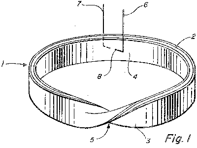
Figure 1 is a perspective view of one embodiment of this invention,
Figure 2 is a cross-sectional view of the Moebius strip showing the location of the resistor, insulator and electrical leads, and
Figure 3 is a cutaway view of a section of a resistor which embodies this invention.
In the embodiment of the invention illustrated in Figure 1 and Figure 2, non-inductive resistor 1 comprises non-conductive ribbon 2 of an insulative material such as Mylar (polyethylene terepthalate) on both sides of which resistive ribbons 3 and 4 have been applied. Resistive ribbons 3 and 4 can be made of a resistive material such as Tophet A (80 Ni, 20 Cr) or for very low resistance, aluminum. The combined ribbons, 2,3, and 4 are then twisted as shown at point 5 and resistive ribbon 3 connected to a resistive ribbon 4 such as by soldering so as to form a Moebius strip. Resistive ribbons 3 and 4, when connected form a single Moebius surface. Electrical leads 6 and 7 are then attached such as by soldering to diametrically opposite points 8 and 9 of resistive ribbons 3 and 4 to complete the resistor.
It is understood that the resistive ribbons 3 and 4 may be replaced by resistive wire such as Manganin (84 Cu, 12 Mn, 4 Ni) bifilar wire wherein the insulation normally provided would replace non-conductive ribbon 2. By bifilar wire, it is meant two parallel strands of wire covered by and separated by the same insulator. The spacing between the wires provided by the insulation should be maintained when the respective wires are connected together to form the Moebius strip so as to have minimum reactance in the resistor.
In operation, a high frequency electrical current inserted across electrical leads 6 and 7 will travel in opposite directions between the leads through resistive ribbons 3 and 4. The electromagnetic fields generated by these currents thereby cancel each other resulting in an essentially non-inductive, non-reactive resistor as shown in Table 1.
Table 1 ~
Conductor Resistance (ohms) Reactance (200 kc) Resistive material
Ribbon 12.7 0.0305 microhenries Tophet A
Ribbon 80 0.1 picofarad Tophet A
Wire 50.3 0.090 microhenries Manganin
Wire 62 0.069 picofarad ManganinThe Moebius resistor listed first in Table 1 was pulsed at 1000 volts and had a measured rise time of 0.1 microsecond.
It was found that the reactance and/or resistance of a resistor embodying this invention was unaffected by handling or changes in form. Once the resistor is connected as described above in a Moebius strip, the resistor need not be maintained in any particular form such as that shown in Figure 1 but can be wound around a cylindrical core or a card or for that matter rolled in a ball providing the resistive ribbons are insulated from each other as is well known in the art. A Moebius strip resistor was wound on a cylindrical core without any effect to its operation thereby enabling compact packaging of the resistor.
Further, as shown in Figure 3, two sets of resistive ribbons 10 and 11 and 12 and 13 respectively were applied side by side on the same non-conductive ribbon 14 with about 1/16 inch spacing and the combined unit connected as described with respect to Figure 1 so as to form two Moebius strip resistors using ribbons 10 and 11 as one resistor and ribbons 12 and 13 as the other resistor. These resistors were then connected successively in series and in parallel and measurement made of the resulting resistance and reactance. It was found that the resultant resistance value changed in accordance with the usual series-parallel effect without changing the time constant from that of a single resistor. Thus, a group of Moebius strip resistors can be arranged for most any resistance value either by series connection or parallel connection and still maintain the time constant. Since these resistors can be wound around any form and not change the reactance, a group of resistors can be made on the same ribbon and the combined resistor wound around a common form with a comparable size to present resistors.
It will be understood that various changes in the details, materials and arrangements of the parts, which have been herein described and illustrated in order to explain the nature of the invention may be made by those skilled in the art within the principles and scope of the invention as expressed in the appended claims.
What is claimed is:
(1) A non-inductive electrical resistor comprising in combination, a ribbon of non-conductive material having opposite surfaces defining a continuous uniform surface in the form of a Moebius strip, at least a single uniform layer of resistive material disposed in continuous manner circumferentially throughout and in parallel coextensivity on said opposite surfaces, and a pair of electrical leads connected to the layer of resistive material at points aligned with each other on opposite surfaces of the non-conductive material.
(2) The combination of claim 1 in which the resistive material comprises a plurality of resistive layers and each layer is uniformly and continuously disposed throughout and in parallel coextensivity on the said opposite surfaces.
(3) The combination of claim 2 in which each resistive layer has a pair of electrical leads connected thereto at points aligned with each other on opposite surfaces of the non-conductive material.