Evan
REED, et al.
Shocked Salt - Coherent Light
Shocked Salt - Coherent Light
Evan Reed
reed23@llnl.gov
https://www.llnl.gov/news/newsreleases/2006/NR-06-01-03.html
Jan 13, 2006
Livermore
researchers find new source of coherent light
LIVERMORE, Calif. — With the exception of lasers and free-electron lasers, there hasn’t been another fundamental way to produce coherent light for close to 50 years.
But a group of researchers from Lawrence Livermore National Laboratory and the Massachusetts Institute of Technology have found a new source of coherent optical radiation that is distinct from lasers and free-electron lasers.

Emission
of coherent light at 22 THz
This figure shows the emission of coherent light at 22 THz from a molecular dynamics simulation of shocked NaCl (table salt). The left panel shows the emission of the light as a function of time while the shock is propagating. The right panel shows the generated radiation as a function of location within the shocked crystal indicating the 22 THz coherent signal is generated at the shock front (between the white dotted lines).
This figure shows the emission of coherent light at 22 THz from a molecular dynamics simulation of shocked NaCl (table salt). The left panel shows the emission of the light as a function of time while the shock is propagating. The right panel shows the generated radiation as a function of location within the shocked crystal indicating the 22 THz coherent signal is generated at the shock front (between the white dotted lines).
Applications for this research are numerous, but the most immediate result may be a new diagnostic tool to determine the properties of shock waves, said Evan Reed, an E.O. Lawrence postdoctoral fellow at Lawrence Livermore and lead author of a paper that appears in the Jan. 13 edition of Physical Review Letters.
Through a series of theoretical calculations and experimental simulations, scientists generated a mechanical shock wave inside a dielectric crystalline material, in this case kitchen salt (NaCl). One might expect to see only incoherent photons and sparks from the shocked crystal.
But what they found was so much more. Weak yet measurable coherent light was seen emerging from the crystal. The emission frequencies are determined by the shock speed and the lattice make-up of the crystal.
The team found that measurable coherent light can be observed emerging from the crystal in the range of 1 to 100 terahertz (THz).
“To our knowledge, coherent light never has been seen before from shock waves propagating through crystals because a shocked crystal is not an obvious source to look for coherent radiation,” Reed said. “The light and radiation was in a portion of the electromagnetic spectrum that is not usually observed in these types of experiments.”
Coherent light is very narrow bandwidth radiation; it is useful for interferometry (the measurement of two or more waves coming together at the same time and place, such as optical and shock waves) and is usually associated with lasers.
The invention of the laser in 1958 as a source of coherent light enabled a wide range of applications including medical technologies and energy production because of the coherence of the light they generate. However, producing coherent light from a source other than a laser can serve as a diagnostic for understanding shock waves, specifically providing information about shock speed and the degree of crystallinity, Reed said.
In the computational experiments, the researchers observed the light generated by a shocked polarized material by performing molecular dynamics simulations of shock waves propagating through crystalline NaCl. The simulations solved the classical equations of motion for atoms that are subject to interaction, thermal effects and deformation of the crystal lattice. The intensive computer simulations were made possible by utilizing LLNL’s Thunder parallel computer.
Other Livermore authors include Richard Gee of LLNL’s Chemistry and Chemical Engineering Division.
LLNL’s Laboratory Directed Research and Development program is funding an experiment to observe coherent radiation in the laboratory. Reed, Michael Armstrong (a Chemistry and Materials Science postdoctoral researcher) and researchers from Los Alamos National Laboratory (LANL) will collaborate on the project, which will be conducted at LANL experimental facilities.
Founded in 1952, Lawrence Livermore National Laboratory has a mission to ensure national security and apply science and technology to the important issues of our time. Lawrence Livermore National Laboratory is managed by the University of California for the U.S. Department of Energy’s National Nuclear Security Administration.
Lawrence
Livermore Laboratoery S&TR ( Nov 2006 )
A Shocking New Form of Laserlike Light
by
Ann Parker
[ PDF ]

Researchers at Livermore and the Massachusetts Institute of Technology will use this experimental apparatus to attempt to produce coherent light
from mechanically shocked crystals.
Physical Review Letters, January 11, 2006
Volume 96 ( 1 ) - Abstract
Coherent
Optical Photons from Shock Waves in Crystals
Evan J. Reed1,2,*, Marin Soljacic1, Richard Gee2, and J. D. Joannopoulos1
1Center for Materials Science and Engineering and Research Laboratory of Electronics, Massachusetts Institute of Technology, Cambridge, Massachusetts 02139, USA
2Lawrence Livermore National Laboratory, Livermore, California 94551, USA
11 January 2006
We predict that coherent electromagnetic radiation in the 1–100 THz frequency range can be generated in crystalline materials when subject to a shock wave or solitonlike propagating excitation. To our knowledge, this phenomenon represents a fundamentally new form of coherent optical radiation source that is distinct from lasers and free-electron lasers. The radiation is generated by the synchronized motion of large numbers of atoms when a shock wave propagates through a crystal. General analytical theory and NaCl molecular dynamics simulations demonstrate coherence lengths on the order of mm (around 20 THz) and potentially greater. The emission frequencies are determined by the shock speed and the lattice constants of the crystal and can potentially be used to determine atomic-scale properties of the shocked material.
http://www.aip.org/pnu/2006/split/761-4.html
Number 761 #4, January 11, 2006
Shock-Produced
Coherent Light
by
Phil Schewe and Ben Stein
by
Phil Schewe and Ben Stein
Physicists at MIT and Livermore National Lab have discovered a new source of coherent radiation distinct from traditional lasers and free-electron lasers; they propose to build a device in which coherent photons are produced by sending shock waves through a crystal. The result would be coherent light resembling the radiation issuing from a laser; but the mechanism of light production would not be stimulated emission, as it is in a laser, but rather the concerted motion of row after row of atoms in the target crystal.
The passing shock front, set in motion by a projectile or laser blast, successively excites a huge density wave in the crystal; the atoms, returning to their original places in the matrix, emit light coherently, mostly in the Terahertz wavelength band. Although sources of coherent light in this part of the electromagnetic spectrum have developed in recent years, it is still a difficult task.
The next step will be to carry out an experimental test of the shock-wave light production. This work will be performed at two national labs -- Livermore and Los Alamos. According to Evan Reed (who moved from MIT to Livermore, reed23@llnl.gov) the first likely application of coherent radiation will be as a diagnostic for understanding shock waves. The radiation should provide information about shock speed and the degree of crystallinity.
http://www.nature.com/news/2006/060116/full/news060116-7.html
18 January 2006
Get
laser-like beams from salt
by
Philip Ball
by
Philip Ball
Could laser-like light be squeezed from salt?Could laser-like light be squeezed from salt model suggests that shocking a crystal will produce synchronized light.
Physicists in the United States have discovered a way to make what is essentially laser light, without using a laser. All you need to do, they say, is give a crystal of table salt a sharp knock.
It was previously assumed that this would do nothing more than squeeze sparks and ordinary light out of the crystal. But Evan Reed of the Lawrence Livermore National Laboratory in California and his co-workers say that the shock will also generate a small amount of 'coherent' light1, the stuff that comes from lasers.
This unexpected source of laser-like light is not just an academic oddity. The new work shows that the coherent light coming from shocked salt should be in a fequency band called terahertz radiation, which cannot be generated by ordinary lasers, says Marin Soljacic, one of Reed's collaborators.
Terahertz radiation, with wavelengths of about a millimetre to tens of micrometres, is increasingly in demand for biomedical and technological applications. In particular, the radiation can peer through human flesh to image the anatomy beneath, without harming tissues the way X-rays do.
You might not get much of this kind of light out of a grain of salt, the team notes. But it could also provide a useful diagnostic tool for studying the effects of shock waves on crystalline materials, says Soljacic, who is based at the Massachusetts Institute of Technology (MIT).
The light fantastic
“The big difficulty is detecting it.”
Light is composed of packets of energy called photons, each of which can be described as a wave with a particular frequency and wavelength. In ordinary (incoherent) light, like that from a light bulb, these waves rise and fall independently of one another. In coherent light, on the other hand, the waves are all synchronized, rather like a group of soldiers marching in step.
It is this characteristic that gives laser light its special properties. The beam stays bright and does not spread out, for example, enabling the fine focus necessary in CD and DVD players.
Making coherent light in lasers is a feat of coordination: all the photons are released together thanks to a positive feedback process through which one photon stimulates the release of another. This process gives 'laser' its name: it's an acronym of Light Amplification by Stimulated Emission of Radiation.
Reed and colleagues say that the coherence of light emitted from a shocked crystal comes instead from the way that a shock wave passing through the material can induce the regular rows of atoms to move in synchrony. This motion produces an electromagnetic wave - in other words, light.
Look and you shall find
Countless experiments have investigated the effects of shock waves on materials; the Lawrence Livermore lab is one of the world leaders in this area. But Reed's team says that coherent light emission has never been seen before, simply because no one thought to look for it.
His team tested their idea in a computer model, which predicted how sodium chloride (common salt) should behave when exposed to the kind of shock wave produced by an explosion or a bright laser pulse. The result was spikes of radiation emitted at extreme-infrared (terahertz) frequencies, corresponding to bands of coherent emission.
So much for the theory; will it work in practice? Reed says he is hoping to find out, in an experimental collaboration between the Livermore lab and Los Alamos National Laboratory in New Mexico. "The big difficulty is detecting the coherent signal. It'll be relatively weak," explains his MIT colleague John Joannopoulos.
Massachsuetts Institute of Technology
References
Reed E. J., et al. Phys. Rev. Lett., 96. 013904 (2006).
US7116458
COHERENT GENERATION, CONVERSION, OR MODULATION OF ELECTROMAGNETIC RADIATION USING SHOCK WAVES OR SOLITIONS PROPAGATING THROUGH EXCITONIC OR POLARITONIC CRYSTALS
COHERENT GENERATION, CONVERSION, OR MODULATION OF ELECTROMAGNETIC RADIATION USING SHOCK WAVES OR SOLITIONS PROPAGATING THROUGH EXCITONIC OR POLARITONIC CRYSTALS
An optical modulator includes a crystal structure that exhibits polaritonic or excitonic behavior. A shock wave propagates through the crystal structure so as to corehently generate, convert or modulate electomagnetic radiation from the terahertz to the x-ray ranges.
PRIORITY INFORMATION
[0001] This application claims priority from provisional application Ser. No. 60/551,127 filed Mar. 8, 2004, incorporated herein in its entirety.
BACKGROUND OF THE INVENTION
[0002] The invention relates to the field of optical modulators, and in particular to a method of modulating light utilizing shock waves in a crystal structure.
[0003] There are very few ways to generate and manipulate coherent radiation. The generation of coherent radiation is imperative for interferometry and other important optical techniques. Existing practical sources of coherent radiation are quantum lasers and free electron lasers. The technology presented in accordance with the invention represents a new source of coherent radiation.
[0004] Uses for terahertz radiation range from the new field of THz spectroscopy, to fundamental studies of phonon
dynamics, to an alternative to harmful x-rays in medical imaging to security screening devices able to penetrate clothing to detect explosives or other weapons. However, the generation of narrow bandwidth radiation in the terahertz regime has proven to be a difficult task. While substantial progress has been made, existing sources of THz radiation have substantial shortcomings that limit their practical use.
[0005] Generally, existing techniques are limited to 1-10 microwatt power outputs, requiring long exposure times for probing. Quantum cascade lasers can be used to generate narrow bandwidth coherent THz radiation, but must be cooled below room temperature and are limited to frequencies above about 2 THz. Photoconductive approaches can generate only broad bandwidth THz radiation up to around 2 THz and require cooling the photoconductive element below room temperature.
[0006] Nonlinear frequency downconversion approaches can provide coherent radiation but are also limited in their efficiency, providing power outputs in 1-10 microwatt range.
SUMMARY OF THE INVENTION
[0007] According to one aspect of the invention, there is provided an optical modulator that includes a crystal structure that exhibits polaritonic or excitonic behavior. A shock wave propagates through the crystal structure so as to optically modulate and manipulate a light signal propagating in the crystal structure.
[0008] According to another aspect of the invention, there is provided an optical isolator that includes a crystal structure that exhibits polaritonic or excitonic behavior. A shock wave propagates through the crystal structure so as to optically modulate and manipulate a light signal propagating in the crystal structure.
[0009] According to another aspect of the invention, there is provided a method of modulating a light signal. The method includes providing a crystal structure that exhibits polaritonic or excitonic behavior. Also, the method includes propagating a shock wave through the crystal structure so as to optically modulate and manipulate a light signal propagating in the crystal structure.
BRIEF DESCRIPTION OF THE DRAWINGS
[0010] FIG. 1 is a schematic diagram of a shock wave moving to the right which increases the resonant frequency of the polarizable elements as it propagates;


[0017] The invention relates to how light can be modulated and manipulated when coupled to polaritonic and excitonic phenomena in materials containing a shock wave or shock-like propagating excitation. Theoretically predicted effects include the conversion of an applied static electric or magnetic field to coherent terahertz or optical frequency radiation and anomalous Doppler-like frequency shifts that are orders of magnitude larger than the usual Doppler shift and can be used for coherent frequency conversion.
[0018] The coherence arises in a classical fashion, in distinction to the quantum origin of coherence present in lasers. This technology represents a fundamentally new form of coherent light source. The frequency shifts are of a linear nature, distinguishing them from the usual nonlinear approaches to frequency conversion. The linearity results in intensity independent conversion efficiencies. This disclosure also details how light of optical or terahertz frequencies can be used to resolve and probe dynamical atomic scale phenomena. A nanoscale optical isolator can be constructed using this technology.
[0019] Utilizing the invention, one can show that coherent terahertz and optical radiation can be generated when a shock wave or shock-like excitation propagates through a crystal of classical polarizable electric dipoles. Many materials exhibiting polaritonic or excitonic behavior are examples of such a system. Coherent terahertz or optical frequency radiation can be generated under certain circumstances. An existing terahertz or optical frequency signal can be coherently converted to another frequency through an anomalously large Doppler-like effect. This frequency conversion effect is orders of magnitude larger than the usual Doppler shift from the moving shock wave or shock-like wave. Such a shock-like time-dependent effect can be utilized as an opto-isolator with physical size orders of magnitude smaller than the wavelength of the light on which it operates. Miniaturization of optical-isolation systems is one of the biggest challenges to optical integration.
[0020] These new predicted effects are observable using a variety of experimental techniques. Planar shock waves can be generated using high intensity pulsed lasers. Shock fronts generated using this technique have been measured to have thicknesses of less than a few tens of crystal lattice planes. An application of the new physics in this work is the measurement of the shock front thickness with precision greater than achievable with current x-ray techniques. Such measurement constitutes ultra sub-wavelength resolution of dynamical phenomena, resolving atomic scale phenomena with light of wavelength orders of magnitude longer. Surface plasmons are another excitation that can be coupled to light to observe these predicted effects. A variety of experimental techniques can be utilized to observe these effects in surface plasmon systems.
[0021] Coherent x-rays are extremely difficult to generate using existing techniques. Approaches that do not involve the detonation of nuclear weapons (x-ray laser) are extremely inefficient (high-harmonic generation). The technology presented in this disclosure may be used to produce coherent x-rays.
[0022] To explore the phenomena associated with light scattering from a shocked polaritonic or excitonic material, perform finite-difference time-domain simulations of Maxwell's equations in one dimension, single polarization, and normal incidence. A polarizable element [mathematical formula - see original document]
Here, [mu]n(t)=vn(t)2 where is the polarizability, v is the volume associated with each polarizable element, n(t) is the resonant frequency of the nth polarizable element, and is a damping term. Equation 1 is solved together with Maxwell's equations in ID, [mathematical formula - see original document]
where [Omega] corresponds to the pre-shock state, is the shift in across the shock front 2 [beta] and vs is the shock speed.
[0023] The observation of some effects can be demonstrated in computer simulations of the model given above. Generation of coherent radiation can be generated from a zero frequency input signal (constant electric or magnetic field) in an insulator or by flowing a current through a metal. Consider a shock wave that propagates through an insulator. As the shock compresses the material, the resonant frequency of polarizable elements within the material can either increase or decrease depending on the material and the particular polarizable elements. In this scenario, one can consider a system where the resonance frequency of the polarizable elements increases upon shock compression. The resonant frequency of the polarizable elements in this scenario is depicted in FIG. 1.
[0024] FIG. 1 shows a schematic diagram of a shock wave moving to the right which increases the resonant frequency of the polarizable elements as it propagates. The resonant frequency of the polarizable dipoles is on the low frequency side of the polaritonic bandgap. Suppose a constant electric or magnetic field is applied throughout the material while the shock wave is propagating. This uniform field induces some moment in the polarizable elements that is emitted as multiple coherent higher frequencies when the resonant frequency of the polarizable elements is increased by the shock.
[0025] FIG. 2 shows results of an FDTD simulation for the scenario in FIG. 1 when the shock propagates with a speed of vs=3.3*10<-5 > c/a which is a typical shock speed of about 10 km/sec. The resonant frequency of the polarizable dipoles ranges from 0.15*10<-4 > c/a in front of the shock to 1.15*10<-4 > c/a behind the shock and the loss parameter=10<-5 > c/a. The polarizability a/v=4.4*10<3 > in front of the shock and a/v=76 behind the shock. The shock front thickness is 20a. FIG. 2 shows the absolute value of the Fourier transform of the magnetic field H over the time interval t=7.5*10<5 > a/c. During this time interval, the shock front is located is located in the vicinity of x/a=125 and travels a distance of approximately 25a.
[0026] Transmitting boundary conditions exist on the left and right sides of the computational cell at x/a=0 and x/a=200. There are several finite elements with no polarizability (vacuum) at the edges of the computational cell. A small amount of emitted light may be reflected from the dielectric mismatch at this interface and propagate back toward the shock as would occur under experimental conditions. A current source at x=9a with zero frequency is slowly turned on at the start of the simulation (before the time interval for the Fourier transform of FIG. 2 begins.) This source generates a constant magnetic field throughout the computational cell.
[0027] As the polarizable elements are moved up in frequency by the shock compression, radiation is re-emitted at multiple discrete frequencies. The emitted radiation is of a coherent nature if the input signal is coherent. Since the input frequency is zero in this case, long time coherence of the input signal is trivial to realize. The number of frequencies emitted from the shock depends an a variety of factors which include the shock front thickness, the polarizability, the magnitude of the resonant frequency shift of the polarizable elements, and the amount of absorption in the polarizable elements.
[0028] FIG. 2 corresponds to an experimentally realizable situation. For example, if the lattice constant a=10 A. The polarizable dipoles vary in frequency from 4.5 THz in front of the shock to 35 THz behind the shock. The generated radiation has frequencies of 10 and 20 THz. The frequency of the generated radiation can be varied by using a crystal with a different periodicity or sound speed because the frequencies generated in this case are approximately generated [omega]generated=vs/a 1, where 1 is a positive integer. Shock front thicknesses of tens of lattice units or less are readily achievable experimentally.
[0029] A remarkable property of this frequency generation effect is that the efficiency is independent of the amplitude of the input signal. This is a result of the fact that this is a linear system, distinguishing it from the usual methods of optical frequency conversion involving the use of materials with a nonlinear optical response. In these systems great care must be taken to ensure input intensities are high enough and phase matching constraints are achieved to obtain sufficient conversion efficiency. The intensity of emitted radiation can potentially be quite high because of the ease with which large polarization fields are created at small frequencies. If the area of the shock wave is 100*100 [mu]m an each polarizable element contains an energy of about 0.1 eV, the shock can generate radiation with an power up to 103 Watts. The efficiency of the effect increases with increasing polarizability, decreasing losses and decreasing initial lower bandgap edge.
[0030] This technology also represents a fundamentally new way to study crystallography. Crystallography is currently studied with x-rays. The technology presented here enables the study of crystal structure by monitoring the spatial and frequency dependence of emitted THz radiation when a shock or soliton propagates through the crystal.
[0031] One can consider a scenario where the input signal has a non-zero frequency. A material is utilized where the polarizable elements of an insulating material move down in frequency when compressed by the shock wave, as in FIG. 3. Consider radiation incident from the right (in the pre-shock region.) As the shock wave propagates, this radiation couples into the polarizable elements and moves down in frequency until it escapes to the right at a lower frequency.
[0032] FIG. 4 shows a computer simulation of the scenario in FIG. 3. The absolute value of the Fourier transform of the magnetic field for is shown. The shock wave moves through about x/a=25 during the Fourier transform time interval. The resonant frequency of the polarizable dipoles (green dotted line) is on the low frequency side of the polaritonic bandgap. Radiation incident from the right resonantly couples into the polarizable dipoles which move down in frequency before re-emitting the radiation. The magnitude of the frequency shift in this reversed Doppler effect is several orders of magnitude larger the normal Doppler shift from an object moving at the shock speed. The re-radiated radiation is coherent if the input signal is coherent. A similar scenario can occur if the frequency of the polarizable dipoles increases upon compression.
[0033] In FIG. 4, the resonant frequency of the polarizable elements decreases from 3.5*10<-4 > c/a in front of the shock to 2.5*10<-4 > c/a behind the shock and the loss parameter y=10<-5 > c/a . The polarizability is a/v =8 in the pre-shock region and v=16 in the post-shock region. The shock propagates with a speed of vs=3.3*10<-5 > c/a which is a typical shock speed of about 10 km/sec. The shock front thickness is 20a.
[0034] Moreover, FIG. 4 shows the absolute value of the Fourier transform of the magnetic field H over the time interval t=7.5*105 a/c. During this time interval, the shock front is located is located in the vicinity of x/a=125 and travels a distance of approximately 25a. Transmitting boundary conditions exist on the left and right sides of the computational cell at x/a=0 and x/a=200. A small amount of emitted light can be reflected from the dielectric mismatch at this interface and propagate back toward the shock as would occur under experimental conditions. A current source at x=191a with frequency v=3*10<-4 > c/a is slowly turned on at the start of the simulation (before the time interval for the Fourier transform of FIG. 4 begins.) FIG. 5 shows the absolute value of the Fourier transform of the polarization field P for the simulation of FIG. 4. The shock wave moves through about x a=25 during the Fourier transform time interval. The resonant frequency of the polarizable dipoles is on the low frequency side of the polaritonic bandgap. Radiation incident from the right resonantly couples into the polarizable dipoles which move down in frequency before re-emitting some of the radiation. Losses decrease the magnitude of the polarization as the polarizable dipoles move down in frequency. FIG. 6 shows a simulation where multiple frequencies are reflected by the shock. This simulation is similar to that shown in FIGS. 4 and 5.
[0035] FIG. 6 shows the absolute value of the Fourier transform of the magnetic field H over the time interval t=7.5*10<5 > a/c. During this time interval, the shock front is located is located in the vicinity of x/a=125 and travels a distance of approximately 25a. Transmitting boundary conditions exist on the left and right sides of the computational cell at x/a=0 and x/a=200. A small amount of emitted light may be reflected from the dielectric mismatch at this interface and propagate back toward the shock as would occur under experimental conditions. A current source at x=191a with frequency v=3.5*10<-4 > c/a is slowly turned on at the start of the simulation (before the time interval for the Fourier transform of FIG. 6 begins.)
[0036] In FIG. 6, the resonant frequency of the polarizable elements decreases from 4*10<-4> c/a in front of the shock to 0 (metallization) behind the shock and the loss parameter [gamma]=2*10<-5 > c/a . The polarizability is [alpha]/v=6.2 in the pre-shock region. The shock propagates with a speed of vs=3.3*10<-5 > c which is a typical shock speed of about 10 km/sec. The shock front thickness is 20a.
[0037] The simulations in the figures in this section are experimentally realizable. For example, in FIG. 6 if the lattice constant a=10 A, the dipoles vary have frequency of 120 THz in the unshocked material. The generated radiation has frequencies separated by 10 THz. The loss parameter in this simulation has the property that [mathematical formula - see original document]
0.05 which is typical of an excitonic or polaritonic excitation.
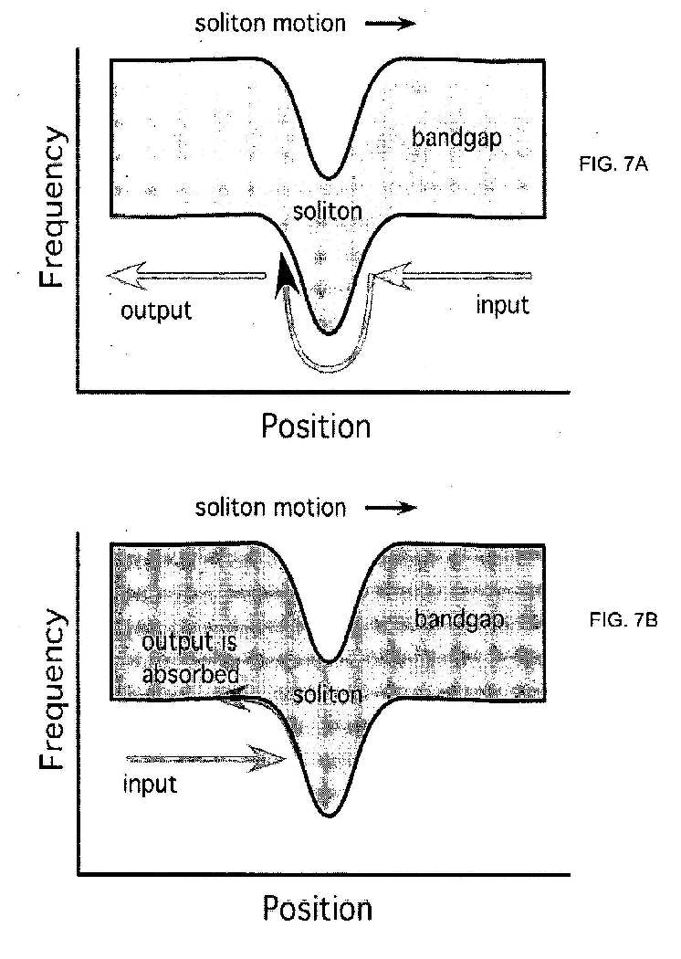
[0038] The lack of a sufficiently miniaturized technique for optical isolation presents one of the biggest challenges to optical integration. One can show how a propagating soliton-like pulse in the polarization resonance frequency can be utilized as an optical isolator. Light that is incident from the right is allowed to propagate through the device with some degree of attenuation, while light incident from the left is completely absorbed by the device. The physical size of the solitonic pulse required for such a device is orders of magnitude smaller than the wavelength of the light and is ideal for optical integration.
[0039] FIGS. 7A-7B show schematic diagrams of the frequency of the polaritonic or excitonic bandgap as a function of position. As the soliton propagates, it changes the resonant frequency of the polarizable elements. The pulse propagates to the right. FIG. 7A shows how light of some input frequency incident from the right can be transmitted through the soliton by coupling into and back out of the resonant elements. FIG. 7B shows how light of the same frequency incident from the left will be couple into the polarizable elements and never couple back out. The light in this case is absorbed by losses in the polarizable elements. This system represents a nanoscale optical isolator because the soliton can be of atomic spatial dimensions and light is only allowed to propagate from left to right through the system.
[0040] The lowest frequency of the soliton must be within a few vs/a of the incident frequency to prevent re-emission of the absorbed radiation to the left. The incident frequency must be within vs/a of the bottom of the bandgap to ensure that the radiation from the left is absorbed instead of being re-emitted to the left. Some losses occur in the transmission scenario in the top figure. If the optical system is not sensitive to frequencies sufficiently different from the input frequency, these frequency criteria are not required. These losses are expected to depend on the spatial dimensions of the soliton, amount of intrinsic loss in the polarizable elements, and shock speed.
[0041] In a practical device, a means of repetitive generation of such solitonic pulses is also required, which would likely be the largest component of the system and the key factor in the suitability for optical integration. Solitonic pulses of the type discussed here can be generated using ultrashort pulsed lasers.
[0042] The new physical phenomena presented herein can all be understood within the context of several analytical theories and qualitative arguments.
[0043] The effects predicted are observable in materials that are not perfect crystals. In polycrystalline materials, additional frequency components are expected to be within the emission spectrum. In any real crystalline material, defects exist that diminish the crystalline properties. It is believed that the presence of defects will result in emission at frequencies other than those at which the perfect crystal emits. In liquids or amorphous materials, non-coherent emission in a broad bandwidth may occur. If the frequency shift of the polarizable elements is sufficiently large, the bandwidth of emitted radiation in this case is limited by the shock front thickness and rate of damping of the polarizable elements. This property could be used as a diagnostic tool for determination of the shock front thickness in shock wave experiments.
[0044] Atomic scale resolution of the front thickness can be determined to a degree better than is possible with current x-ray technology. It can be possible to measure the temperature of a material behind the shock front by measuring the emission from thermally populated polarizable elements as a second shock wave propagates through the material behind the first shock wave. This technology also represents a new diagnostic tool for the study of material solitons.
[0045] Dispersion in phonon bands can be neglected in polaritonic systems because the shock speed is considerably faster than optical phonon speeds. This may not hold in excitonic systems, but no bands are expected to exist in sharp shock fronts where the frequencies of polarizable elements are sufficiently different to prevent exciton transport. The effects presented in this disclosure are expected to be observable when the shock wave propagates off-axis to the crystal. This scenario is not a ID scenario. Thermal effects can also diminish coherence properties, but the polarization due to the electromagnetic radiation can be made considerably larger than polarization due to thermal effects.
[0046] An additional embodiment of this invention is to utilize surface plasmons as the polarizable elements. Surface plasmons are charge density waves that propagate at the interface between a metal and a dielectric material. The resonant frequency of surface plasmons can be varied in a shock-like fashion by modulating the dielectric of the dielectric material in a shock-like fashion, either by sending a physical shock through the dielectric or through other means of modulation. It is also likely possible to observe the effects presented here in systems that do not involve physical shock waves. For example, the generation and manipulation of coherent x-rays may be possible if the resonant frequency of the polarizable dipoles can be changed by a pulse of light propagating through a material. In this case, the generated frequencies are on the order of 10<4 > eV if v c and a 1[deg.]A. Atomic core electronic states may be utilized as the polarizable elements in this scenario. Coherent x-rays are extremely difficult to generate using existing techniques. Approaches that do not involve nuclear weapons (x-ray laser) are extremely inefficient (high-harmonic generation). The technology described here can be utilized to generate coherent phonons, which can be used for a variety of purposes including nanoscale imaging.
[0047] Although the present invention has been shown and described with respect to several preferred embodiments thereof, various changes, omissions and additions to the form and detail thereof, may be made therein, without departing from the spirit and scope of the invention.
PRIORITY INFORMATION
[0001] This application claims priority from U.S. provisional patent application Ser. No. 60/464,006 filed on Apr. 18, 2003, and is a continuation-in-part of U.S. patent application Ser. No. 10/412,089 filed on Apr. 11, 2003.
BACKGROUND OF THE INVENTION
[0002] The invention relates to the field of photonics and, in particular, to photonic crystals. Photonic crystals are a promising and versatile way to control the propagation of electromagnetic radiation. Nevertheless, very little attention has been given to the effects of non-stationary photonic crystals on electromagnetic radiation propagation. It has been shown that the frequency of light can be changed across a bandgap in a photonic crystal which is physically oscillating. However, the frequency of oscillation is required to be of the order of the bandgap frequency in the photonic crystal. Such oscillation frequencies are impossible for light of 1 [mu]m wavelength.
[0003] There is no known non-quantum mechanical way to significantly narrow the bandwidth of a wavepacket by an arbitrary amount and change the frequency of light to an arbitrary amount with high efficiency. Acousto-optical modulators can change the frequency by a part in 10<-4> , but larger changes in frequency are desirable for most applications. Non-linear materials can be used to produce large changes in light frequencies with less than perfect efficiency. For example, if light of frequencies [omega]1 and [omega]2 is shined into a non-linear material, light of frequencies [omega]1+[omega]2 and ¦¦[omega]1-[omega]2¦¦ may be produced. In addition to the less than perfect conversion efficiencies of these techniques, the frequencies produced are still limited by the range of input frequencies. Production of an arbitrary frequency is not possible unless an arbitrary input frequency is available. Furthermore, great care must be taken in the design of the device to ensure momentum conservation, which is required for high efficiency. Additionally, high intensities are required, and the frequencies produced are still limited by the range of input frequencies and phase-matching constraints. Using such prior art systems, production of an arbitrary frequency shift in a given system is not possible.
[0004] Of additional interest in optical applications is the ability to trap and manipulate pulses of light. Few technologies exist to trap 100% of the energy of a pulse of light for a period of time which is determined while the light is trapped. Existing approaches for trapping light for a pre-specified amount of time require the use of large lengths (kilometers) of optical fiber. The time required for light to propagate through the fiber is a function of the length. A number of large reels of fiber of varied lengths are required to delay light pulses for a range of times, and even then the delay time cannot be determined in real time.
[0005] Photonic crystals have been shown to be a versatile way to control the propagation of electromagnetic radiation. However, very little attention has been given to the effects of non-stationary photonic crystals on electromagnetic radiation propagation.
[0006] Whatever the precise merits, features, and advantages of the above-mentioned approaches, they fail to achieve or fulfill the purposes of the present invention's system and method for trapping light for a controlled period of time via shock-like modulation of the photonic crystal dielectric.
SUMMARY OF THE INVENTION
[0007] According to one aspect of the invention, there is provided a method of modifying frequency of electromagnetic radiation input into a nonlinear medium. The method includes forming a moving grating in the nonlinear medium by introducing at opposite ends of the nonlinear medium a first set of electromagnetic radiation having varying frequencies. Electromagnetic radiation is inputted into the nonlinear medium at a first frequency. Also, the method includes extracting electromagnetic radiation at a second frequency from the nonlinear medium. The moving grating in the nonlinear medium allows for electromagnetic radiation to be modified into the second frequency.
[0008] According to another aspect of the invention, there is provided a method of converting frequency of electromagnetic radiation input into a nonlinear medium. The method includes forming a moving grating in the nonlinear medium by introducing at opposite ends of the nonlinear medium a first set of electromagnetic radiation having varying frequencies. Electromagnetic radiation is inputted into the nonlinear medium at a first frequency. Also, the method includes extracting electromagnetic radiation at a second frequency from the nonlinear medium. The moving grating in the nonlinear medium allows for electromagnetic radiation to be converted into the second frequency.
[0009] According to another aspect of the invention, there is provided a device for converting frequency of electromagnetic radiation. The device includes a nonlinear medium that forms a moving grating in the nonlinear medium by introducing at opposite ends of the nonlinear medium a first set of electromagnetic radiation having varying frequencies. Electromagnetic radiation is inputted into the nonlinear medium at a first frequency and extracted at a second frequency from the nonlinear medium. The moving grating in the nonlinear medium allows for electromagnetic radiation to be converted into the second frequency.
BRIEF DESCRIPTION OF THE DRAWINGS
[0010] FIG. 1 illustrates a shock wave profile.

[0012] FIG. 3 illustrates four moments in time in a computer simulation of the shock in FIG. 1.
[0013] FIG. 4 contains results of a simulation similar to that in FIG. 3, but with a faster moving shock front of [nu]=3.4*10<-3 > c.
[0014] FIG. 5 illustrates the results of a simulation wherein the bandwidth of input light is reduced by a factor of 4.
[0015] FIG. 6 illustrates a frequency versus position graph of a broad shock wave propagating to the right of a photonic crystal.
[0016] FIG. 7 illustrates a schematic of a shock wave compressing a material with a spatially dependent bandgap.
[0017] FIG. 8 illustrates a schematic showing how the present invention is used to delay and alter the form of electromagnetic signals.
[0018] FIG. 9 illustrates a scenario wherein electromagnetic energy is shined into a defect band.
[0019] FIG. 10 illustrates a graph of the dielectric as a function of position for three equally-spaced instants of time, t1<t2<t3.
[0020] FIG. 11 shows the effect of this dielectric on a Gaussian pulse, which propagates toward the moving interface from the uniform dielectric region.
[0021] FIG. 12 illustrates how light of a single frequency is split into multiple discrete frequencies.
[0022] FIG. 13 illustrates a device comprising two different photonic crystals which shifts light upwards in frequency.
[0023] FIG. 14 illustrates a device which shifts light down in frequency, wherein the device is designed so that the light does work on the photonic crystal on the right.
[0024] FIG. 15 represents a combination of the devices of FIGS. 13 and 14.
[0025] FIG. 16 gives a schematic of a possible all optical switch based on the present invention.
[0026] FIG. 17 illustrates the effects of a strategically placed moving reflecting surface in a photonic crystal on the electromagnetic radiation inside.
[0027] FIG. 18 presents a specific example of how a signal can be transferred from one wavelength to another using a thin reflecting film as an intermediary.
[0028] FIG. 19 is a schematic diagram of the invention using moving gratings.
[0029] FIG. 20 is a time graph showing the movement of the moving gratings in a nonlinear material.
[0030] FIG. 21 is a graph demonstrating the operations of the invention.
[0031] FIG. 22 is a simulation result illustrating a constant electric field applied in the linear region.
DETAILED DESCRIPTION OF THE INVENTION
[0032] Although the present invention has been shown and described with respect to several preferred embodiments thereof, various changes, omissions, and additions to the form and detail thereof may be made therein without departing from the spirit and scope of the invention.
[0033] The effects on electromagnetic radiation propagating in a shocked photonic crystal (consisting of alternating dielectric layers along a particular direction) are considered. Finite difference time domain (FDTD) simulations of Maxwell's Equations in one dimension, single polarization, and normal incidence for a system described by a time-dependent dielectric [epsilon](x,t) are used to explore the phenomena associated with light scattering from a shock-wave, or shock-like wave, in a photonic crystal.
[0034] A typical shock wave profile is depicted in FIG. 1. It corresponds to the dielectric function given by [mathematical formula - see original document] where [nu] is the shock speed and [alpha] is the period of the pre-shocked crystal. The photonic crystals on both sides of the shock front have periodic variations of [epsilon] ranging from 1 to 13. The thickness of the shock wave front is given by [gamma]<-1> , which is 0.05. FIG. 1 describes this shock wave propagating to the right (leaving a compressed lattice behind) in the dielectric described by Equation (1) as a function of position for three equally-spaced instants of time t1<t2<t3. Arrows follow the shock front and material paths, which move at different speeds. The shocked lattice is identical to the original but with a smaller lattice constant. In this case, the shock wave compresses the lattice by a factor of 2. The interface moves at the shock speed [nu] and the material behind also moves uniformly at a slower speed-known as the particle speed. In this case, the particle speed is [nu]/2. This scenario can roughly be thought of as two different lattice constant photonic crystals moving toward each other.
[0036] The shock wave profile of the dielectric constant in the photonic crystal can be generated by a variety of means. One method includes launching a physical shock wave into the photonic crystal using explosive loading, high-intensity lasers or other means. Another method involves the generation of the shock wave profile through the use of materials which change the dielectric constant under an applied electric field or applied change in temperature. Some of these materials can be modulated at GHz frequencies with 1% changes in the refractive index. A generalized idea of a shock wave can be adopted as a dielectric modulation which is steady in a reference frame moving at the shock speed. A time-dependent shock wave profile may be realized by time-dependent modulation of the local dielectric at all points in the system. In addition to a constant shock velocity, a propagation velocity which is time-dependent may provide better results for a particular application. The thickness of the shock wave front may also be varied for desired effect. Other possible ways of producing similar effects in photonic crystals may involve the simultaneous interaction of light with a spinning disk and an object fixed in the laboratory frame. However, the means for producing such shockwaves should not be used to limit the scope of the present invention.
[0037] As an illustrative example, the specific case is considered wherein the shock wave compresses the lattice constant behind the shock by a factor of 2. Additionally, the shock front has a thickness on the order of, or less than, a single lattice constant, as depicted in FIG. 1. The bandgaps for the crystals which exist in front of and behind the shock front are depicted in FIG. 2. It should be noted that there is a complete gap which extends over the entire crystal from frequency [omega]1 to [omega]2.
[0038] First, the effect of electromagnetic radiation in the photonic crystal is considered. Electromagnetic radiation is shined into the crystal in the opposite direction of shock propagation (or in a direction that not necessarily the same as that of the direction of shock propagation) just below the second gap at [omega]1 (e.g., indicated by arrow 202 for [omega]1=0.37) on the right side of FIG. 2. This radiation is converted up in frequency to [omega]2 (e.g., indicated by arrow 204 for [omega]2=0.44), where it propagates away from the shock and can be extracted from the system near the input. Arrows 206 and 208 indicate the adiabatic evolution of the modes for the lowest two bands.
[0039] It should be noted that specific bandgaps (i.e., 1<st > bandgap, 2<nd > bandgap, etc.) are used for illustration
purposes only and the present invention equally applies to the use of other bandgaps. Hence, specific bandgaps should not be used to limit the scope of the present invention.
[0040] FIG. 3 illustrates four moments in time in a computer simulation of the shock in FIG. 1. For example, FIG. 3 shows the magnetic field for a simulation where the shock front (dashed line) propagates to the right, with [nu]=3.4*10<-4 > c. It should be noted that the shock front location is indicated by the dotted line 302. The panels in FIG. 3 are obtained by Fourier transforming the magnetic field over windows of time ([Delta]t=200 [alpha]/c) centered at the times shown in the upper right corners. Light is initially spatially contained in a Gaussian distribution centered around x/[alpha]=40 at the band edge frequency. As the Gaussian distribution moves and broadens to the left, most of the incident light is trapped in a localized state at the shock front in the overlapping bandgap frequency region of the two photonic crystals. While it is trapped, it evolves up in frequency through the pre-shocked bandgap and is released to the right of the shock, with about 20% change in frequency in this case. More specifically, the light begins the simulation below the gap in the unshocked material at [omega]1=0.37 (indicated by arrow 304) and, as the light begins to propagate to the left, most of it is trapped at the shock front until it escapes to the right at [omega]1=0.44 (indicated by arrow 306).
[0041] It should be noted that the amount of frequency shift in this example can be tuned by adjusting the size of the bandgap of the pre-shocked crystal and, hence, such frequency shift amounts should not be used to limit the scope of the present invention.
[0042] The shock wave propagates about 0.5[alpha] in FIG. 3, and this frequency conversion process is observed once for every lattice unit the shock wave traverses, resulting in a pulsed output for a continuous wave input. The pulse rate can be controlled with the shock speed. Qualitatively similar effects were observed for a slower shock velocity of v=3.4*10<-5 > c.
[0043] An additional consequence of this scenario is the localization of light for a controlled period of time. If the speed at which the shock-like interface moves can be controlled, then the light can be confined in the gap region for a time that is determined by that shock speed. It should be noted that the propagation speed of light is near zero while trapped at the shock front, which has useful applications in telecommunications or quantum optics.
[0044] FIG. 4 contains results of a simulation similar to that in FIG. 3, but with a faster moving shock front of [nu]=3.4*10<-3 > c. The frequencies are separated by 2 [pi][nu]/[alpha]. Similar to the example in FIG. 2, light enters at [omega]=0.37 (shown by arrow 402) below the bandgap and is converted up in frequency at the shock front and propagates away as discrete frequencies around [omega]=0.45 (shown by arrow 404). Light in this simulation starts out as a Gaussian centered at x/[alpha]=220 with the bandgap edge carrier frequency. The Fourier transform of magnetic field which produced this figure utilized a longer time period ([Delta]t=6000[alpha]/c) than that of FIG. 3 and shows the entire upconversion of light from below the gap to the top of the gap as the shock front passes through several lattice periods. The light trapped at the shock front appears to exist in discrete frequencies and escapes at the top of the gap in such frequencies. This discretization can be loosely interpreted as a result of repeated bounces of the light between the moving material on the left and the fixed material on the right and is commensurate with the periodic nature of the pulsed output. The interpretation of the output light in FIGS. 3 and 4 as equally-spaced discrete frequencies or pulses is a matter of frequency resolution in the detection apparatus.
[0045] The frequency of the localized state at the shock front observed in FIG. 3 is well defined in the limit of a slowly propagating shock where [mathematical formula - see original document] However, for shock speeds sufficiently fast for this condition to break down, the localized mode possesses an effective bandwidth which is on the order of the bandgap frequency width. FIG. 4 is approaching this regime, where it is almost more appropriate to think of the light continuously moving up through the bandgap rather than in a pulsed fashion as in FIG. 3.
[0047] Additionally, the shock-like dielectric modulation of FIG. 1 is used to narrow the bandwidth of a pulse of light. This is accomplished by confining the light between the moving shock front on the left and a reflecting surface of the right (indicated by arrow 500). FIG. 5 illustrates the results of such a simulation (with the dotted lines 502 and 504 indicate the shock front), where the bandwidth of input light is reduced by a factor of 4 (bandwidth of input light=[Delta][omega]=0.01 and bandwidth of output light=[Delta][omega]=0.0025). In this specific example, the shock is moving, with [nu]=10<-4 > c and [gamma]<-1> =2. The narrowing process can become more effective for slower shock velocities, larger simulation cells, and narrower initial bandwidths.
[0048] Changing the thickness of the shock front has an effect on the frequencies produced and the degree of continuity of the frequency-converted electromagnetic radiation. Continuous frequency conversion is accomplished with a shock wave possessing a front thickness much larger than the lattice spacing. This is depicted in FIG. 6.
[0049] FIG. 6 illustrates a frequency versus position graph of a broad shock wave propagating to the right of a photonic crystal. The shock front width is much larger than the lattice constant. A signal input at [omega]1 from the right (arrow 602) is coherently converted up in frequency to [omega]2 and output to the left (arrow 604). It is also envisioned that coherency may be maintained for small frequency shifts for narrow shocks. It should be noted that running the shock wave in reverse has a frequency lowering effect for light input from the right at [omega]2, which is complimentary to the frequency increasing effect described here.
[0050] While there are numerous ways to increase the bandwidth of a wave packet, there are currently no classical (non-quantum mechanical) ways to decrease the bandwidth. This can be accomplished through the addition of a photonic crystal mirror on the right side of the system in FIG. 2. If electromagnetic radiation of a range of frequencies below [omega]1 is shined into the system, it will be confined between the shock front and the mirror on the right side. As the shock propagates, all this radiation is shifted up in frequency until the lower band edge in the pre-shocked material is reached; then the radiation is shifted up in frequency through the total system gap and can be extracted on the right side.
[0051] Many other methods are envisioned to reduce or increase the bandwidth of a pulse of light based upon this configuration. Some of these are related to the frequency dependence of the Doppler shift and the frequency dependence of the adiabatic evolution of the modes. The rate of adiabatic frequency shift of the modes in the pre-shocked material is a function of frequency. Modes close to the bottom of the gap change frequency more slowly than those away from the gap due to the high density of modes there. This may have bandwidth altering applications. It is also possible to vary the frequency width of the bandgap as a function of position in the crystal to control the density of states, as in FIG. 7.
[0052] FIG. 7 illustrates a schematic of a shock wave compressing a material with a spatially dependent bandgap. All light which exists between [omega]1 and [omega]2 is converted to [omega]2 and escapes on the right side. This will decrease the distance the shock wave must travel to convert all the energy in a given bandwidth.
[0053] Thus, the use of photonic crystals as frequency-dependent mirrors allows for the confinement of light of certain frequencies, while others are allowed to escape. If the geometry of the photonic crystals is sufficiently slowly altered that the confined light changes frequency slowly, it will all escape at the edge of the confining frequency nearly monochromatically. It should be noted that this effect cannot be accomplished with metallic mirrors due to their lack of significant frequency dependence and rapid absorption of electromagnetic energy.
[0054] In addition to frequency changes, the shocked photonic crystal has the capability of trapping light for a period of time in a defect state located at the shock front, as in FIG. 3. While the light is being shifted up in frequency through the gap, it is trapped at the shock front. If the speed of the shock wave can be controlled, then the light in the localized defect state can be trapped there for a controlled time. The light can be released by running the shock forwards or backwards. In the forward case, the light is released at the top of the pre-shocked material gap. In the reverse case, the light is released at the original frequency that it was input. This scheme is an optical pulse delay, which can delay pulses of light "on the fly" by adjusting the shock velocity.
[0055] FIG. 8 illustrates a schematic showing how the present invention is used to delay and alter the form of electromagnetic signals. The electromagnetic trapping effect observed in the shock wave scenario can be generated by a variety of other means. The most obvious is to actually change the distance between two photonic crystals using piezoelectric materials or other means, as in FIG. 1. Another means of generating the appropriate time-dependent effects is through the use of materials which change the dielectric constant under an applied electric field or applied change in temperature. Some of these materials can be modulated at GHz frequencies with 1% changes in the refractive index. Other possible ways of producing similar effects in photonic crystals may involve the simultaneous interaction of light with a spinning disk and an object fixed in the laboratory frame.
[0056] The incorporation of crystal defects and defect bands into the shocked photonic crystal can also have useful properties. For example, consider electromagnetic energy which is shined into a defect band, as depicted in FIG. 9. The shock is propagating to the right and converts all the energy in the defect band up in frequency if the highest group velocity is less than the shock wave speed. If the group velocity of the energy in the defect band is less than the shock speed, then 100% of the energy will be converted in frequency, and can be extracted out the left side in the post-shocked material.
[0057] In addition, if the shock wave changes the amount of dispersion in that band, the frequency bandwidth can be changed by the shock wave. For example, if the shock is run in reverse, it will move the crystal defects apart as it propagates. This decreases the amount of dispersion in the defect band and forces all the light in that band to occupy a narrower bandwidth. Slow separation of the defects to infinity will force all of the light into a single frequency.
[0058] These ideas apply to any system which is described well by tight-binding. For example, efficient frequency conversion can be achieved in this fashion in a series of coupled inductor-capacitor resonators. If the frequency of the resonators is changed more quickly than the group velocity of the energy in the system, then 100% of the input energy will be converted.
[0059] There has been recent interest in nonlinear effects in light trapped in localized states in photonic crystals. The conversion of light from frequency [omega] to 3[omega] can be accomplished more efficiently than usual through the use of such localized states which do not have a well-defined momentum.
[0060] It is possible to achieve large amplitudes localized at the shock front. These large amplitudes are a result of the adiabatic compression of an extended state to a localized state. These amplitudes increase with the size of the system and increase as the shock velocity decreases. Amplitudes of several orders of magnitude higher than the amplitude in the pre-shock region are possible.
[0061] If the intensity of electromagnetic radiation in the defect state at the shock front is sufficiently high that non-linear material effects become important, then light of frequency 3[omega] may be generated, where w is the frequency of the defect state. In this case, as the frequency of the light in the defect state changes, so will the 3[omega] generated by nonlinearities. If 3[omega] is a frequency which coincides with allowed modes of the system, this light will be able to escape the shock front and propagate away.
[0062] In addition to large frequency changes and bandwidth narrowing, it is possible to observe other novel effects in photonic crystals which are modulated in a shock-like pattern. For example, a reverse Doppler shift from a moving boundary in a photonic crystal can be observed using a dielectric of the form [mathematical formula - see original document] This is shown in FIG. 10.
[0064] FIG. 10 illustrates a graph of the dielectric as a function of position for three equally-spaced instants of time, t1<t2<t3. Arrows follow the shock front and material paths, which move at different speeds. In this case, a moving interface exists between a photonic crystal and a uniform dielectric medium and the photonic crystal does not move relative to the uniform medium, but movement of the interface causes an expansion or growth of the crystal region.
[0065] FIG. 11 shows the effect of this dielectric on a Gaussian pulse, which propagates toward the moving interface from the uniform dielectric region. The light is at a frequency where it is completely reflected by the bandgap region of the crystal, and a negative Doppler shift is observed. Here, [gamma]<-1> =1.8, and [nu]=0.125c. A similar simulation was performed for a Gaussian pulse around [omega]=0.19, in which a zero Doppler shift was observed. A positive Doppler shift was observed for incident frequencies between about 0.19 and the top of the reflecting bandgap.
[0066] It is also possible to make light of a single frequency split into multiple discrete frequencies. This is illustrated in FIG. 12. This simulation is similar to that in FIG. 11 except the dielectric in the crystal region has additional high spatial frequency components. The dielectric is [mathematical formula - see original document] with shock front thickness parameter, [gamma]<-1> =0.013 and [nu]=0.025 c.
[0068] The Gaussian pulse incident from the right in FIG. 11 is split into evenly spaced frequencies upon reflection. Some of the light is reflected with no frequency shift. The intensity of each of the reflected frequency components can be controlled by adjusting the form of the dielectric in the crystal region. As in the cases of FIGS. 3 and 4, the interpretation of the reflected light as evenly-spaced discrete frequencies or as a periodic modulation of a single frequency is a matter of experimental timescale resolution.
[0069] The phenomena observed in FIGS. 3 and 4 can be largely understood by considering the time-evolution of the various allowed modes as the shock propagates. Each time the shock wave propagates through one lattice unit, the crystal on the right in FIG. 2 is reduced in length by one lattice unit and the crystal on the left is increased by one lattice unit. Since the number of allowed values of k in a band is equal to the number of lattice periods in the crystal (ignoring polarization degeneracy) each time the shock wave passes over one lattice unit, the number of states in each band in the pre-shocked crystal must decrease by one and increase by one in the post-shocked crystal. This transfer process is indicated by the mode movement arrows in FIG. 2 for the lowest two bands. It should be noted that to accomplish this in the case of the second band, it is necessary for a mode to move up through the overlapping gap formed by the second bandgap in the preshocked region and the first bandgap in the postshocked region.
[0070] Indeed, the large frequency changes in FIGS. 3 and 4 are a direct result of the adiabatic evolution of the light through this overlapping bandgap. The light is essentially trapped in a cavity which is "squeezed" as the shock compresses the lattice, thereby increasing the frequency. This occurs once each time the shock propagates through a lattice unit.
[0071] While a significant change in the frequency of electromagnetic radiation through mechanical means usually requires the interaction with objects that are moving at a significant fraction of the speed of light, the adiabatic approach does not have this requirement. The adiabatic nature of the evolution of the radiation up in frequency through the total system bandgap has the property that it can be arbitrarily slowly completed with the same large shifts in frequency. This key physical mechanism liberates the shocked photonic crystal from the impossible task of interface propagation near the speed of light. Finally, it should be noted that a time-reversed, frequency lowering effect also occurs in this adiabatic picture.
[0072] The adiabatic picture is valid as long as the scattering processes involved with the incident light reflecting from the shock wave do not introduce frequency components that are significantly outside the original input pulse bandwidth. Therefore, the more time the incident light spends interacting with the shock front, the more likely it is for this condition to hold. This condition is satisfied for the systems exemplified in FIGS. 3 and 5, mostly satisfied for the system shown in FIG. 4, and completely invalid for the systems in FIGS. 11 and 12.
[0073] To develop a non-adiabatic theory, a scenario is provided where the incident light is at a frequency that falls within the gap of the compressed crystal. However, the systems depicted in FIGS. 1 and 10 must be treated slightly differently. Let us begin with the case in FIG. 1.
[0074] Far away from the shock front, the electric field in the pre-shocked photonic crystal is given by E(x,t)=E0e<ikx> wk,n(x)e<-i[omega]t> , (4) where k and n denote the translational and band indices, and wk,n(x) has the periodicity of the lattice, wk,n(x+[alpha])=wk,n(x).
[0076] Since the frequency of the incident light lies within the bandgap of the compressed photonic crystal, an effective model of the shock front is a mirror with a space-dependent E field reflection coefficient, R(x), where x is the mirror position. R has the property that R(x)=1, since the incident light reflects from the bandgap of the post-shocked crystal. In general, R has some frequency dependence, but the bandwidth of the incident light is considered sufficiently small to neglect it. If the shock front is stationary, the boundary condition in terms of incident and reflected light is E1e<ik> <1> <x> wk1,n(x)e<-i[omega]> <1> <t> =E0R(x)e<ik> <0> <x> wk0,n(x)e<-i[omega]> <0> <t> , (5) where ko and kl correspond to the incident and reflected states, respectively, and E0 and E1 are constants.
[0078] For light near the band edge at k=0, the frequency has the form [omega]=[omega]0+[alpha]k<2> . This substitution can be made without loss of generality because the condition near any band edge can be obtained by considering k->k-kedge and a redefinition of the function wk,n(x). If an assumption is made that the shock is moving sufficiently slowly that the reflected light has the form of a single Bloch state, then a substitution can be made, x->xo-[nu]t, to obtain a relation for the boundary condition at the shock front. This gives [mathematical formula - see original document] where El(t) now has some amplitude time-dependence due to the term in brackets.
[0080] It can be shown that, near a band edge where k is small, [mathematical formula - see original document] where un(x) has the periodicity of the lattice and is independent of k. Equation (6) can be further simplified by noting that when [mathematical formula - see original document] and, likewise for ko, the term in brackets in Equation 6 is unity, and El(t) is time-independent. Since small k is near the Brillouin zone center, this should be the case most of the time. If R(x)=-1 as for a metallic mirror, the time-dependence of Equation 6 must satisfy, [alpha]k1<2> -[alpha]k0<2> +(k1-k0)[nu]=0. (8) This gives a frequency shift of [mathematical formula - see original document]
[0084] The last relation is given in terms of the group velocity defined by [mathematical formula - see original document] The relation between incident and reflected group velocities can be expressed as [nu]g,l=2[nu]-[nu]g,o. If [nu]<0 and [nu]g,o<0, the mirror is moving to the right and incident light propagates to the left.
[0086] There are two remarkable features of Equation 9. The first is that, in the slow velocity limit where [mathematical formula - see original document] the Doppler shift 2[nu]ko is much smaller in magnitude than the usual vacuum Doppler shift [mathematical formula - see original document] near the Brillouin zone center. The second notable feature is that for [nu]<0, above the bandgap where [alpha]>0 the Doppler shift is positive, whereas below the bandgap where [alpha]>0, the Doppler shift is negative. Therefore, incident light is Doppler shifted away from the bandgap region on both sides of the bandgap.
[0089] It is interesting to note that the term in brackets in Equation (6) changes phase slowly except when [mathematical formula - see original document] when the phase can change very rapidly. This indicates that the reflected frequencies are very sensitive to the position of the reflector in these special regions for light where [mathematical formula - see original document] This property could be useful in resolving the motion of objects which have oscillation amplitudes much smaller than the wavelength of the light they are reflecting, or for mechanical modulation of optical signals.
[0092] Considering the case of FIG. 10 where the pre-shocked material is completely uniform; light in the uniform region that reflects from the photonic crystal region can be endowed with an anomalous Doppler shift, as in FIG. 11, and be split into multiple frequencies, as in FIG. 12.
[0093] It should be noted that it is not possible to observe these effects by simply translating a photonic crystal through a uniform medium because the reflection coefficient for the photonic crystal in that case is constant, as in the case of a metal mirror. The new key physical phenomena that appear in this section result from the fact that the photonic crystal region "grows" into the uniform region, and not merely translates.
[0094] As a simple description of the phenomena in FIGS. 11 and 12, the photonic crystal boundary is represented as a space-dependent reflection coefficient. The reflected light can be expanded in the plane wave solutions of the uniform medium, [mathematical formula - see original document] where R(x) can be written R(x)=[Sigma]G[beta]Ge<-iGx > which is the most general form with the property R(x)=R(x+[alpha]). The reciprocal lattice vectors G are [mathematical formula - see original document] where q is an integer. This substitution and letting x->x0-[nu]t yield a relation required by the time dependence of Equation (10) of, [omega]G+kG[nu]=[omega]0+k0[nu]-G[nu] (11) where the j index has been replaced with the reciprocal lattice vector index G. The reflected frequencies in the non-relativistic limit are, [omega]G-[omega]0=(2k-G)[nu]. (12) The reflected light has frequency components that differ from the usual Doppler shift by the amount G[nu]. For light near the first bandgap frequency, G[nu] is on the order of or larger than the Doppler shift from a metal mirror. The amplitude of each of these components is, EG=[beta]G¦¦E0. (13)
[0099] The reverse Doppler shift scenario in FIG. 11 corresponds to the case where the only dominant component of R(x)=[Sigma]G[beta]Ge<--iGx > is the one corresponding to [mathematical formula - see original document] Equation (12) indicates that the reflected light should have a single frequency with a negative shift if [nu]<0, ko<0, and [mathematical formula - see original document] which is the case in FIG. 11.
[0102] The multiple reflected frequencies of FIG. 12 are also represented by Equation 12. In this case R(x) has several spatial frequency components, which result from the high spatial frequency components in [epsilon](x) for the crystal given by Equation 3. Furthermore, the incident light in the simulation in FIG. 12 has wavevector [mathematical formula - see original document] which is coincident with a value of G for the crystal. Therefore, some of the reflected light has the same frequency as the incident light.
[0104] Equation (12) is based on the assumption of a very sharp shock front. FIG. 10 was produced with a relatively broad shock front width greater than [alpha], which has the effect of suppressing multiple reflected frequencies.
[0105] Consider the non-adiabatic model associated with the scenario of FIG. 1. With the limit [nu]->0, the non-adiabatic
model reduces to the adiabatic limit and provides some new physical insight. As was previously discussed, the adiabatic limit is achievable by increasing the time the incident light spends interacting with the shock front. Therefore, the adiabatic limit is taken by considering the effect of repeated bounces of the light from the slowly moving reflector where each bounce is described by Equation (6). It is envisioned that the light bounces between the slowly moving reflector and a fixed reflector positioned a distance L>>[alpha] in the crystal. Let R(x)[identical to]e<i[theta](x)> , and let the term in brackets in Equation 6 be denoted by e<iP(x> <0> <-[nu]t)> . Assigning unit magnitude for the term in brackets in Equation (6) is acceptable for all time in the limit of small v where kl->ko. Then, the time dependence of Equation (6) requires, [alpha]k1<2> +k1[nu]=[alpha]k0<2> +k0[nu]+[theta]'(x0-[nu]t0)[nu]+P'(x0-[nu]t0)[nu], (14) where [theta] and P have been linearized about t0, which is valid in the limit [nu]->0. Primes denote derivatives. Then, after p bounces off the light between the stationary and moving reflectors, [mathematical formula - see original document]
[0107] The number of bounces of the light p that occur during a time [alpha]/[nu] when the reflector moves through one lattice constant is [mathematical formula - see original document] The variation of [nu]g over this time can be neglected in the limit L>>[alpha].
[0109] Taking the limits [nu]->0 (p->[infinity]) and L<<[alpha] give, [mathematical formula - see original document]
[0110] The periodicity of the crystal gives the property that [theta](x+[alpha])-[theta](x)=2[pi]l, and the periodicity of wk,n gives the property that P(x+[alpha])-P(x)=2[pi]m, where l and m are integers. This substitution and some simplification gives the final result for the adiabatic change in k during the propagation of the shock over one lattice constant, [mathematical formula - see original document]
[0111] The integer m is related to the particular bandgap around which wk,n describes states. It can be shown that for a sinusoidal dielectric, m=-1 above and below the first bandgap, m=-2 above and below the second bandgap, and so on. The integer l is also related to the particular bandgap from which light is reflecting. For a sinusoidal dielectric, l=1 for the first bandgap, l=2 for the second, and so on for the higher bandgaps. While quantum numbers are preserved in an adiabatic evolution, the k values referred to here change during an adiabatic evolution because they are convenient labels, not quantum numbers.
[0112] When Equation (17) is applied to the scenario in FIG. 2, l+m=1-2=-1, which indicates that the k quantum number of light will adiabatically decrease one k quantum for each lattice constant the shock wave moves. This is consistent with the adiabatic picture presented above which shows that one mode of the system must move up through the total system gap per lattice unit the shock traverses in FIG. 2. Furthermore, the invariance of the adiabatic picture to the details of crystal structure provides a general proof that the above statements about m and l hold for all crystals.
[0113] Another interesting case is when the shock interface separates two crystals of differing bandgap sizes such that light near the first bandgap in the pre-shocked crystal reflects from the first bandgap of the post-shocked crystal. In this case, l+m=1-1=0, indicating there is no net Doppler shift for small shock velocities. This absence has been observed in FDTD simulations.
[0114] While there are numerous ways to increase the bandwidth of a wave packet, there are, to our knowledge, currently no non-quantum mechanical ways to decrease the bandwidth. An important implication of this adiabatic evolution of light is that the bandwidth of a pulse of light can be modified in a controlled fashion while bouncing between the moving shock wave and a fixed reflecting surface, as in FIG. 5. Equation (17) indicates the width of a wavepacket in crystal momentum space [delta]k should be preserved after many bounces because every k state moves by the same amount. The dispersion relation near a band edge indicates the bandwidth [delta][omega] for a wavepacket of width [delta]k is a function of k near the band edge, [delta][omega]=2[alpha]k[delta]k. Therefore, the bandwidth of a pulse will be altered as it evolves through k-space during the bouncing. This fact enables the compression of the bandwidth of a pulse of light to a vanishing amount in the limits of a large separation between the two reflecting surfaces and slowly moving shock front.
[0115] In FIG. 5, a wavepacket of mean wavevector k is shifted up in frequency toward the band edge, causing the bandwidth to decrease. The bandwidth is modified without a very large change in average frequency. However, if the wavepacket reaches the band edge, it will be trapped at the shock front and converted up in frequency until it is expelled at the frequency of the top of the bandgap. In this case, there is a large average frequency shift in addition to a narrowing in bandwidth. Both of these effects may have useful applications.
[0116] These new technologies have a wide variety of possible applications. The ability to change the frequency of electromagnetic radiation over a wide frequency range (typically 20% or more) with high efficiency is of significant value in the telecommunications industry. This industry utilizes a frequency range of about 3%.
[0117] The capacity to delay a pulse of light for an amount of time which is determined while delaying has applications in the telecommunications industry. The capacity to reorder portions of optical signals can also have applications in the telecommunications industry.
[0118] The capacity to convert a relatively broad bandwidth of frequencies to a nearly single frequency may have applications for the harnessing of solar energy. Current solar cells do not have the capacity to harness all frequency regions of the solar spectrum with high efficiency. A material with an electronic optical bandgap of a given frequency must be fabricated to harness the solar energy in the region of that frequency. Fabrication of such materials is currently not possible for the entire solar spectrum. The devices presented here allow the conversion of parts of the solar spectrum which may not be utilized by solar cells to a frequency which is efficiently converted to electricity. It is envisioned that this results in considerable increases in efficiency of solar cells.
[0119] The perfect absorption of a portion of the electromagnetic spectrum using these devices may be suited to applications where electromagnetic absorption is important.
[0120] Some of the new physical phenomena presented in this paper are most pronounced for light close to the edge of a bandgap where group velocities are small. Group velocities two orders of magnitude less than that in air have been experimentally realized in photonic crystals.
[0121] The generalized shock-like profiles of the dielectric discussed here could be generated by a variety of means. Materials which undergo a change in the dielectric constant under an applied electric field or applied change in temperature are promising candidates. Such an approach might make possible the control of the shock velocity and shock front thickness through time-dependent control of the local dielectric at all points in the system. It is also possible to launch a physical shock wave into the photonic crystal using explosive loading, high-intensity lasers, or other means. The phenomena in FIGS. 11 and 12 should be observable using this approach. Although large compressions are used to illustrate the phenomena in FIGS. 3 and 4, it should be noted that it is possible to observe the same phenomena with compressions of a few percent or less by considering the use of deliberately designed defect bands or overlapping bandgaps formed by higher frequency bandgaps in the pre- and post-shocked crystals.
[0122] Additionally, although this disclosure describes shock-like dielectric modulations, the observed phenomena can be observed in two and three dimensions and using other types of dielectric modulation. MEMS devices provide an avenue for the generation of time-dependent effects in photonic crystals. For example, the adiabatic transfer of light between the bottom and top of a bandgap may be accomplished by varying the air spacing between two photonic crystals of differing lattice constants in an oscillatory fashion. As another example, consider a rotating disk containing a spiral photonic crystal pattern. Small millimeter diameter MEMS disks have been made to rotate at millions of RPM in microengines. Light reflecting from the edge of such a disk will see a dielectric modulation identical to that of FIG. 10 as viewed in a reference frame where the shock front is stationary. Hence, various embodiments are envisioned using variations on this approach. Finally, small time-dependent changes in the dielectric can also be generated using non-linear materials. As examples of specific applications, an optical switch based on the present invention and a method for electromagnetic wave modulation and control through time-dependent photonic crystals are described below.
[0123] FIG. 13 illustrates a device comprising two different photonic crystals which shifts light upwards in frequency. FIG. 14 illustrates a device which shifts light down in frequency, wherein the device is designed so that the light does work on the photonic crystal on the right. If the photonic crystal on the right acts like an oscillation in position, energy is transferred to this oscillator as the conversion process proceeds. In principle, this energy can be extracted through the use of piezoelectric materials or other means.
[0124] While the force felt by a reflecting surface reflecting a beam of light is ordinarily very small, this force is enhanced by many orders of magnitude in devices utilizing the teachings of the present invention. It is estimated that the forces supplied by light are of sufficient magnitude to displace a typical MEMS device on the order of 10% of the wavelength of 1.55 [mu]m light for intensities in the 10 milliwatt range. This allows for the possibility to control the geometry of MEMS devices with light.
[0125] FIG. 15 represents a combination of FIGS. 13 and 14. Light of frequency [omega]0 is shined into the system from
right and left. When the center photonic crystal moves to the left, the light on the right is shifted down in frequency and the light on the left is shifted up in frequency. The system is designed so that the force supplied by the light on the right is greater than the force on the left. As a consequence of this, more energy must be extracted from the light which is shifted down than put into the light which is shifted up if the right and left inputs are of the same intensity. If the center crystal is mounted on an effective spring, it will return to and past its original position and the conversion process will begin again.
[0126] As a consequence of the ability to change the geometry of MEMS devices with light using our technology, an all optical switch can be produced. FIG. 16 gives a schematic of a possible all optical switch. The input and output waveguides are coupled with a high Q cavity. The resonant frequency of the cavity can be controlled by changing the geometry. If the resonant frequency is close to the frequency of the input light, resonant tunneling can occur and 100% transmission can be achieved. This has been previously demonstrated in photonic crystal systems.
[0127] If light which is shined into the gate waveguide gets trapped in a high-pressure state, the high Q cavity geometry may be altered. It is thus possible to turn the device on using only light. If the gate light source disappears, the device may still remain in the on configuration if light is still trapped in the high pressure state. The length of time the device stays in the on configuration will depend on the device design and the intensity of the initial gate pulse and the absorption coefficient of the photonic crystal material and the Q of the high pressure state.
[0128] As mentioned above, another example as the present invention's application is a method for electromagnetic wave modulation and control through time-dependent photonic crystals. FIG. 17 illustrates the effects of a strategically placed moving reflecting surface in a photonic crystal on the electromagnetic radiation inside.
[0129] There exist special places in a photonic crystal near a band edge where the phase of reflected light is a strong function of the velocity of the reflecting surface. These special locations exist in the neighborhood of places where dH/dx=0, where H is the magnetic field. If a reflecting surface, such as a mirror or another photonic crystal, is moved in the vicinity of these locations, an unusually large frequency shift of the reflected light may be observed. The presence of extra frequencies in the reflected signal is a form of modulation.
[0130] FIG. 17 presents a 1-dimensional schematic of the utilization of this phenomenon. As the mirror 1702 on the left moves, light incident from the right is modulated as it is reflected. Hence, light which is incident from the right at a frequency just below the bandgap in the photonic crystal is reflected from the mirror. If the mirror is moving, a large Doppler shift is observed in the reflected light. This frequency shift or broadening is a modulation of the reflected light. This device allows the resolution of changes in location of the mirror on the left much less than the wavelength of the light shined in from the right in FIG. 17. FIG. 18 presents a specific example of how a signal can be transferred from one wavelength to another using a thin reflecting film as an intermediary. A signal on the left modulates the displacement of the thin film which modulates the light of a different frequency on the right side. This scenario is identical to FIG. 17 with the exception of the electromagnetic signal incident from the left which can be a source of modulation of the reflecting surface through photon pressure. The device of FIG. 18 allows for modulating a signal with another of different frequency.
[0131] Applications which require resolution of reflecting objects which move length scales much less than the wavelength of the probe light can benefit from this technology. Miniaturized motion detectors for MEMS devices could be constructed. Additionally, this method of modulation is not bandwidth limited. The direct modulation of optical frequencies with signals that have a broad bandwidth can be accomplished using our invention. This can be very difficult to accomplish using electronics.
[0132] Hence, the present invention's devices allow the generation of an arbitrary frequency, which is tunable by adjusting the size of a bandgap. Generation of an arbitrary frequency through existing means is difficult and costly. The strong interaction of light and matter through the high pressure modes outlined here provides an alternating to nonlinear material effects which require high intensities and electronics which translate optical signals into mechanical effects. Frequency conversion can be accomplished through the present invention's devices without any supplied power or electronics. The perfect absorption of a portion of the electromagnetic spectrum using these devices may be suited to applications where electromagnetic absorption is important. The conversion of electromagnetic energy directly into mechanical energy may have applications in the solar power industry.
[0133] FIG. 19 shows another approach in utilizing moving photonic crystals to achieve highly efficient frequency conversion of electromagnetic radiation. In particular, FIG. 19 shows a material 2 having a nonlinear dielectric response, and a material 6 having a linear response. Electromagnetic radiation of frequencies [omega]1 and [omega]2 are shined in opposite directions. This creates a moving periodic modulation or moving grating of the dielectric, or moving photonic crystal 4, within the nonlinear region. Electromagnetic radiation to be frequency converted is shined from the linear region at a frequency [omega]3. The frequencies [omega]1 and [omega]2 are chosen so that [omega]3 coincides with a bandgap frequency region of the moving photonic crystal in the nonlinear material. The input signal [omega]3 signal has an exponentially decaying spatial dependence into the nonlinear region and is reflected from the moving photonic crystal and propagates away to the right at frequency [omega]4.
[0134] Note [omega]3 falls within one of the bandgaps of the moving photonic crystal 4. The efficiency of this conversion in a phase matched system is 100% for light of bandwidths below the bandgap size of the moving photonic crystal, which can be about 10<-3> [omega]0 in practice. This method of frequency conversion can be performed on arbitrarily weak input signals. In addition to efficient frequency conversion, this technology may also have useful applications for quantum information processing due to the capability to manipulate low intensity signals combined with the preservation of signal bandwidth.
[0135] This embodiment of the invention is a special case of 4-wave mixing where the input signal exhibits an exponentially decaying spatial dependence in the nonlinear region.
[0136] FIG. 20 shows the dielectric at three equally-spaced instants in time, t1>t2>t3. The arrows show the movement of the photonic crystal 4 in the nonlinear material 2.
[0137] If the nonlinear material 2 utilized possesses a nonlinearity with a timescale fast enough to respond to the frequency [omega]1-[omega]2 but slow enough to average over [omega]1+[omega]2 then the interference of the pump beams [omega]1 and [omega]2 produces a grating of lattice constant. [mathematical formula - see original document] with moving velocity [mathematical formula - see original document] where n is the refractive index of the nonlinear material, assumed to be independent of frequency in this case. The input frequency [omega]3 must satisfy, [omega]3 l[omega]2 Eq. 20 where l is a positive integer that corresponds to the particular bandgap from which the incident light reflects. This is an approximate relation because the photonic crystal bandgap has some non-zero width in frequency space. For this input frequency, the output frequency is, [omega]4 l[omega]1 Eq. 21 The amount of frequency shift is given by [mathematical formula - see original document] When l=1 (input signal light reflects from the lowest frequency bandgap), the pump frequencies are equivalent to the input signal and output signal frequencies. The amount of frequency shift relative to the input frequency is given by, [mathematical formula - see original document]
[0143] Analytical theory predicts that there is only one reflected frequency in the limit of a narrow photonic crystal bandgap. This fact enables 100% efficiency in the conversion process. In practice, the small bandgap in the nonlinear material is well into the single reflected frequency regime.
[0144] The previous results were derived using Galilean relativity, which holds correct when v<<c. Relativistic effects can be derived and shown to result in the production of extra reflected frequency components.
[0145] FIG. 21 shows results of a computer simulation illustrating operation of the device. Light is incident to the left at frequency [omega]=0.01. The linear-nonlinear interface is at x=30a, where a is the lattice constant of the photonic crystal. Light is reflected from the interface and propagates to the right at multiple frequencies. The number of reflected frequencies will be 1 in the limit of a small photonic crystal bandgap, as will exist in practical setups. The simulations reported here utilize time-dependent modulations of the index in the nonlinear region, removing lo the need for the pump beams in the simulations. The simulations also possess perfect phase matching, i.e. the dielectric constant exhibits no frequency dependence.
[0146] Under certain conditions, [Delta][omega]/[omega] in Eq. 23 can be made infinite. In this case the input frequency is zero (i.e. a constant electric field). Computer simulation of this scenario is shown in FIG. 22. In FIG. 22, a constant electric field is applied in the linear region. This is upconverted to multiple equally spaced frequencies of similar intensity. Here the dielectric used is given in FIG. 20, and the velocity has been chosen to make the denominator of Eq. 23 is zero. Maximum frequency produced in this scenario is extremely sensitive to the bandwidth of the input signal in this case. It is also sensitive to the frequency dependence of the dielectric which can have an effect on the degree of phase matching.
[0147] This scenario requires the grating to be moving at the speed of light in the nonlinear material, so only one pump frequency [omega]1 is required in this case. A fast nonlinear response can be required to produce a periodic index modulation that is sufficiently fast to observe nonlinear effects in this case. Nonlinear response times on the femtosecond time scale exist in AiGaAs and other materials with a non-resonant excitation. This timescale is fast enough to observe the effects.
[0148] In this embodiment of the invention, it is described in 1D, but higher spatial dimensions can be exploited. For example, the input frequency [omega]3 can be shined on the linear-nonlinear interface at an angle. Since the bandgap frequency of the photonic crystal in the nonlinear material is a function of this angle, the angle can be varied to obtain high conversion efficiency rather than vary the frequencies of [omega]1 and/or [omega]2.
[0149] The bandwidth region where 100% frequency conversion is obtained depends on the power of the beams used to generate the moving grating in the nonlinear material. The typical bandwidth where 100% conversion efficiency can be obtained with the new approach can be up to 10<-3 > [omega]0, where [omega]0 is the average frequency to be converted. These bandwidths are determined by the degree of material nonlinearity and the intensity of the light used to generate the moving grating.
[0150] The exponentially decaying nature of the converted light within the photonic bandgap frequency region in the photonic crystal in FIG. 19 results in a small device. The localization length of light in the photonic crystal is typically between 10<3> [lambda] to 10<4> [lambda] where [lambda] is the wavelength of light to be converted. Some existing approaches to nonlinear frequency conversion require the use of kilometer lengths of fiber to obtain reasonable efficiencies. This exponentially decaying spatial dependence of light in the nonlinear region may also decrease the importance of any phase mismatches that can prevent efficient conversion.
[0151] Although the present invention has been shown and described with respect to several preferred embodiments thereof, various changes, omissions and additions to the form and detail thereof, may be made therein, without departing from the spirit and scope of the invention.
WO2004092819
FREQUENCY CONVERSION BASED ON FOUR-WAVE MIXING
FREQUENCY CONVERSION BASED ON FOUR-WAVE MIXING
A device for converting frequency of electromagnetic radiation includes a nonlinear medium (2) that forms a moving grating (4) in the nonlinear medium by introducing at opposite ends of the nonlinear medium a first set of electromagnetic radiation having varying frequencies (W1, W2). Electromagnetic radiation (W2) is inputted into the nonlinear medium at a first frequency and extracted at a second frequency (W4) from the nonlinear medium. The moving grating in the nonlinear medium allows for electromagnetic radiation to be converted into the second frequency.