Anthony
SUTERA, et al.
Spray-On Antenna
Spray-On Antenna
MATERIAL USED FOR PROPAGATION, EMISSION & ABSORPTION OF EM RADIATION -- WO2012078362 // US2012146855
Nano-Copper
Nano-Antennas
http://news.cnet.com/8301-17938_105-57376903-1/spray-on-antenna-wireless-in-a-can/
February 13, 2012
Spray-on
antenna: Wireless in a can
by Amanda Kooser
by Amanda Kooser

(Credit: Video screenshot by Amanda Kooser/CNET)
It sounds like a particularly suspicious late-night infomercial: Spray your way to a better wireless signal! Improve your range! Save battery! Transmit over great distances under water!
But Chamtech's spray-on antenna is a real product with some impressive claims. It can be sprayed on almost any surface, even trees and orange barrels. It doesn't suck up power. It works in a mysterious nanotech way.
Here's how I imagine the antenna process goes:
Step 1: Spray antenna material on surface.
Step 2: Connect phone to material.
Step 3: ????
Step 4: Make a phone call to the moon.
Chamtech co-founder Anthony Sutera imagines a world where wireless antenna towers are replaced with nano-paint on walls, and issues like iPhone Antennagate are a thing of the past.
"We have come up with a material that when you spray it on, it lays out just in the right pattern and all of these little capacitors charge and discharge extremely quickly in real time and they don't create any heat," Sutera says in a video presentation about the product.
One of Chamtech's tests turned an RFID chip with a 5-foot range into an RFID chip with a 700-foot range. The company lists a spray antenna kit on its site, but pricing for the public is not revealed. The U.S. government is reportedly already playing with the new material.
If all these claims bear out, then I can see everybody wanting to get their hands on a fresh can full of antenna. My only question is where in the grocery store it will be stocked: with the spray cheese or with the gold food paint?
http://www.neowin.net/news/the-amazing-spray-on-antenna
12 February 2012
The
amazing spray-on antenna
by
Tyler Holman
by
Tyler Holman
Wouldn't it be great if you could just pop out a can of spray-on antenna and boost your signal whenever it was running low? Chamtech Enterprises is hoping to make that dream a reality, and if you happen to work for the government, it already is, according to Chamtech's Solve for X presentation.
Chamtech took to Google's Solve for X to show off the new technology. The company plans to turn its focus towards mobile phones and medical devices, offering a quick solution to boosting signals from existing antennas, or creating new ones. Chamtech's 'antenna in a can' is far more efficient than traditional antenna models, offering energy savings equal to 12 times the amount of energy generated by solar and wind in the US annually - and it even works great underwater.
A traditional antenna would require thousands of watts to send out a signal with a one mile range underwater. Chamtech's can do that with only three watts, and have a stronger signal to boot. So how does all of this work?
The truth is, we don't really know. According to Chamtech's co-founder Anthony Sutera, he and his team came up with it in his living room two years ago. It works by manipulating magnetic and radio signals through mysterious organic materials, and you can spray it on any virtually any surface and hook into it with a flexible circuit cable.
According to Sutera, the US government has had a lot of success with the technology, getting better performance out of it than their existing portable antennas, which he described as some of the best around. With the efficiency and mobility offered, it could even be used to rapidly deploy new infrastructure in disaster areas.
Sutera and chief technology officer Rhett Spencer have coated their car antennas with the stuff, boasting that they can now listen to radio stations in Salt Lake City fifty miles away, with 10,000-foot mountain range in between. Within a few months, they hope to be thinking about financing the company, and are looking at venture capital options to help them bring their technology to you.
For his part, Spencer can't wait. “Can you imagine the infrastructure side of things? Telecomm under the oceans, Internet infrastructure, ships and satellite communications in the sea– they can do it out under the water.” Check out video of Chamtech's Solve for X presentation below.
http://www.youtube.com/watch?feature=player_embedded&v=4efE_gO9lFo
http://chamtechops.com/news/
Chamtech
/ Sutera Patents
MATERIAL USED FOR AT LEAST ONE OF PROPAGATION, EMISSION AND ABSORPTION OF ELECTROMAGNETIC RADIATION
WO2012078362
US2012146855
An antenna system and method for fabricating an antenna are provided. The antenna system includes a substrate (310) and an antenna. The antenna includes a conductive particle based material (320) applied onto the substrate (310). The conductive particle based material (320) includes conductive particles and a binder. When the conductive particle based material (320) is applied to the substrate (310), the conductive particles are dispersed in the binder so that at least a majority of the conductive particles are adjacent to, but do not touch, one another.
CROSS-REFERENCE TO RELATED APPLICATIONS
[0001] This application claims the benefit under 35 U.S.C. $119(e) of a U.S. provisional patent application filed on Nov. 22, 2010 in the U.S. Patent and Trademark Office and assigned Ser. No. 61/416,093, a U.S. provisional patent application filed on Apr. 8, 2011 in the U.S. Patent and Trademark Office and assigned Ser. No. 61/473,726, a U.S. provisional patent application filed on Apr. 20, 2011 in the U.S. Patent and Trademark Office and assigned Ser. No. 61/477,587, and a U.S. provisional patent application filed on Aug. 2, 2011 in the U.S. Patent and Trademark Office and assigned Ser. No. 61/514,435, the entire disclosure of each of which is hereby incorporated by reference.
BACKGROUND OF THE INVENTION
[0002] 1. Field of the Invention
[0003] The present invention relates to techniques for a material used for at least one of propagation, emission and absorption of electromagnetic radiation. More particularly, the present invention relates to techniques for a conductive particle based material used for at least one of propagation, emission and absorption of electromagnetic radiation.
[0004] 2. Description of the Related Art
[0005] A conventional antenna is a device with an arrangement of one or more conductive elements that are used to generate a radiating electromagnetic field in response to an applied alternating voltage and the associated alternating electric current, or can be placed in an electromagnetic field so that the field will induce an alternating current in the antenna and a voltage between its terminals. The conductive elements employed in the conventional antenna are typically fabricated from solid metallic conductors. However, the use of solid metallic conductors is limiting.
[0006] Therefore, a need exists for an improved material used for at least one of propagation, emission and absorption of electromagnetic radiation, and implementations of the improved material.
SUMMARY OF THE INVENTION
[0007] An aspect of the present invention is to address at least the above-mentioned problems and/or disadvantages and to provide at least the advantages described below. Accordingly, an aspect of the present invention is to provide techniques for a conductive particle based material used for at least one of propagation, emission and absorption of electromagnetic radiation.
[0008] In accordance with an aspect of the present invention, an antenna system is provided. The antenna system includes a substrate and an antenna. The antenna includes a conductive particle based material applied onto the substrate. The conductive particle based material includes conductive particles and a binder. When the conductive particle based material is applied to the substrate, the conductive particles are dispersed in the binder so that at least a majority of the conductive particles are adjacent to, but do not touch, one another.
[0009] In accordance with another aspect of the present invention, an antenna enhancer system is provided. The antenna enhancer system includes an antenna and an antenna enhancer. The antenna enhancer includes a conductive particle based material. The antenna enhancer is disposed adjacent to and offset from the antenna. The conductive particle based material comprises conductive particles and a binder. When the conductive particle based material is disposed adjacent to and offset from the antenna, the conductive particles are dispersed in the binder so that at least a majority of the conductive particles are adjacent to, but do not touch, one another.
[0010] In accordance with yet another aspect of the present invention, a method for fabricating a conformable antenna is provided. The method includes selecting a substrate on which to fabricate an antenna, selecting a template corresponding to an antenna design, the template comprising one or more cut out portions, applying a conductive particle based material, through the one or more cutout portions of the template, and onto the substrate to form the antenna, and fixing a coupler of a feed line to the antenna. The conductive particle based material comprises conductive particles and a binder. When the conductive particle based material is applied to the substrate, the conductive particles are dispersed in the binder so that at least a majority of the conductive particles are adjacent to, but do not touch, one another.
[0011] Other aspects, advantages, and salient features of the invention will become apparent to those skilled in the art from the following detailed description, which, taken in conjunction with the annexed drawings, discloses exemplary embodiments of the invention.
BRIEF DESCRIPTION OF THE DRAWINGS
[0012] The above and other aspects, features, and advantages of certain exemplary embodiments of the present invention will be more apparent from the following description taken in conjunction with the accompanying drawings, in which:
[0013] FIG. 1 is a captured image of a conductive particle based material according to an exemplary embodiment of the present invention;


DETAILED DESCRIPTION OF EXEMPLARY EMBODIMENTS
[0023] The following description with reference to the accompanying drawings is provided to assist in a comprehensive understanding of exemplary embodiments of the invention as defined by the claims and their equivalents. It includes various specific details to assist in that understanding but these are to be regarded as merely exemplary. Accordingly, those of ordinary skill in the art will recognize that various changes and modifications of the embodiments described herein can be made without departing from the scope and spirit of the invention. In addition, descriptions of well-known functions and constructions are omitted for clarity and conciseness.
[0024] The terms and words used in the following description and claims are not limited to the bibliographical meanings, but, are merely used by the inventor to enable a clear and consistent understanding of the invention. Accordingly, it should be apparent to those skilled in the art that the following description of exemplary embodiments of the present invention are provided for illustration purpose only and not for the purpose of limiting the invention as defined by the appended claims and their equivalents.
[0025] It is to be understood that the singular forms "a," "an," and "the" include plural referents unless the context clearly dictates otherwise. Thus, for example, reference to "a component surface" includes reference to one or more of such surfaces.
[0026] As used herein, the term "substantially" refers to the complete or nearly complete extent or degree of an action, characteristic, property, state, structure, item, or result. For example, an object that is "substantially" enclosed would mean that the object is either completely enclosed or nearly completely enclosed. The exact allowable degree of deviation from absolute completeness may in some cases depend on the specific context. However, generally speaking the nearness of completion will be so as to have the same overall result as if absolute and total completion were obtained. The use of "substantially" is equally applicable when used in a negative connotation to refer to the complete or near complete lack of an action, characteristic, property, state, structure, item, or result.
[0027] As used herein, the term "about" is used to provide flexibility to a numerical range endpoint by providing that a given value may be "a little above" or "a little below" the endpoint.
[0028] As used herein, the term "antenna" refers to a transducer used to transmit or receive electromagnetic radiation. That is, an antenna converts electromagnetic radiation into electrical signals and vice versa. Electromagnetic radiation is a form of energy that exhibits wave-like behavior as it travels through space. In free space, electromagnetic radiation travels close to the speed of light with very low transmission loss. Electromagnetic radiation is absorbed when propagating through a conducting material. However, when encountering an interface of such a material, the electromagnetic radiation is partially reflected and partially transmitted there-though. Herein, exemplary embodiments of the present invention described below are directed toward techniques that allow for a more efficient interface by reducing the reflections at the interface.
[0029] In addition, exemplary embodiments of the present invention described below relate to techniques for a conductive particle based material used for at least one of propagation, emission and absorption of electromagnetic radiation. While the techniques for the conductive particle based material may be described below in various specific implementations, the present invention is not limited to those specific implementations and is similarly applicable to other implementations.
[0030] An initial overview of the conductive particle based material is provided below and then specific implementations in which the conductive particle based material is employed are described in detail further below. This initial overview of the conductive particle based material is intended to aid readers in understanding the conductive particle based material that is the basis of various exemplary implementations, but is not intended to identify key features or essential features of those various exemplary implementations, nor is it intended to limit the scope of the claimed subject matter.
Conductive Particle Based Material
[0031] In one exemplary embodiment, a conductive particle based material is employed. The conductive particle based material includes at least two constituent components, namely conductive particles and a binder. However, the conductive particle based material may include additional components, such as at least one of graphite, carbon (e.g., carbon black), titanium dioxide, etc.
[0032] The conductive particles may be any conductive material, such as silver, copper, nickel, aluminum, steel, metal alloys, carbon nanotubes, any other conductive material, and any combination thereof. For example, in one exemplary embodiment, the conductive particles are silver coated copper. Alternatively, the conductive particles may be a combination of a conductive material and a non-conductive material. For example, the conductive particles may be ceramic magnetic microspheres coated with a conductive material such as any of the conductive materials described above. Furthermore, the composition of each of the conductive particles may vary from one another.
[0033] The conductive particles may be any shape from a random non-uniform shape to a geometric structure. The conductive particles may all have the same shape or the conductive particles may vary in shape from one another. For example, in one exemplary embodiment, each of the conductive particles may have a random non-uniform shape that varies from conductive particle to conductive particle.
[0034] The conductive particles may range in size from a few nanometers up to a few thousand nanometers. Alternatively, the conductive particles may range in size from about 400 nanometers to 30 micrometers. The conductive particles may be substantially similar in size or may be of various sizes included in the above identified ranges. For example, in one exemplary embodiment, the conductive particles are of various sizes in the range of about 400 nanometers to 30 micrometers. Herein, when a range of sizes of the conductive particles are employed, the distribution of the sizes may be uniform or non-uniform across the range. For example, 75% of the conductive particles may be a larger size within a given range while 25% of the conductive particles are a smaller size.
[0035] An effective amount of conductive particles are included relative to the binder so that the conductive particles are dispersed in the binder. The conductive particles may be randomly or orderly dispersed in the binder. The conductive particles may be dispersed at uniform or non-uniform densities. The conductive particles may be dispersed so that at least a majority of the conductive particles are closely adjacent to, but do not touch, one another.
[0036] The binder is used to substantially fix the conductive particles relative to each other and should be a non-conductive or semi-conductive substance. Any type of conventional or novel binder that meets these criteria may be used. The non-conductive or semi-conductive material of the binder may be chosen to function as a dielectric with a given permittivity.
[0037] The conductive particle based material may be formed as a rigid or semi-rigid structure. For example, the conductive particle based material may be a plastic sheet having the conductive particles dispersed therein. The conductive particle based material may be clear or opaque, and may include any shade of color.
[0038] In addition, the conductive particle based material may be a liquid, paint, gel, ink or paste that dries or cures. Here, the binder may include distillates, hardening agents, or solvents such as a Volatile Organic Compound (VOC). In this case, the conductive particle based material may be applied to a substrate. Also, when the conductive particle based material is a liquid, paint, gel, ink or paste that dries or cures, the binder may adhere to the substrate. The conductive particle based material may be spayed on, brushed on, rolled on, ink-jet printed, silk screened, etc. onto the substrate. The use of the conductive particle based material that is a liquid, paint, gel, ink or paste that dries or cures is advantageous in that the conductive particle based material may be thinly applied to a substrate and conform to the surface of the substrate. This allows the conductive particle based material to occupy very little space and, in effect, blend into the substrate.
[0039] The substrate may be the surface of any conductive, non-conductive or semi-conductive substance. The substrate may be rigid, semi-flexible or flexible. The substrate may be flat, irregularly shaped or geometrically shaped. The substrate may be paper, cloth, plastic, polycarbonate, acrylic, nylon, polyester, rubber, metal such as aluminum, steel and metal alloys, glass, composite materials, fiber reinforced plastics such as fiberglass, polyethylene, polypropylene, fiberglass, textiles, wood, etc.
[0040] The substrate may have a coating applied thereto. The coating may be a conductive, non-conductive or semi-conductive substance. The coating may be a paint, gel, ink, paste, tape, etc. The coating may be chosen to function as a dielectric with a given permittivity.
[0041] At least one of a protective and concealing (or decorative) coating may be applied over the conductive particle based material once it has been applied to a substrate.
[0042] An example of the conductive particle based material is described below with reference to FIG. 1.
[0043] FIG. 1 is a captured image of a conductive particle based material according to an exemplary embodiment of the present invention.
[0044] Referring to FIG. 1, the conductive particle based material includes conductive particles and a binder. The conductive particles are randomly shaped, sized and located. However, conductive particles are dispersed so that at least a majority of the conductive particles are closely adjacent to, but do not touch, one another.
[0045] Herein, without intending to be limiting, for a conductive particle based material of a given density of conductive particles, the conductive particle based material may be applied at a thickness such that the conductive particles are dispersed in the binder so that at least a majority of the conductive particles are closely adjacent to, but do not touch, one another. Herein, without intending to be limiting, it has been observed that a conductive particle based material has a resistance of about 3-17 ohms across any given two points on the surface.
[0046] Herein, without intending to be limiting, it has been observed that when the conductive particle based material is formulated such that the conductive particles are dispersed in the binder so that at least a majority of the conductive particles are closely adjacent to, but do not touch, one another, the conductive particle based material exhibits properties that enable it to at least one of efficiently propagate electromagnetic radiation, efficiently absorb electromagnetic radiation from space, and efficiently emit electromagnetic radiation into space. Moreover, it has been observed that those properties may be either supplemented or enhanced by including an effective amount of carbon, such as carbon black, in the conductive particle based material. For example, an effective amount of carbon black may be an amount that corresponds to about 1-7% of the conductive particles included in the conductive particle based material.
[0047] Without intending to be limiting, it is believed that when electromagnetic radiation is introduced into the conductive particle based material, electromagnetic radiation may pass from conductive particle to conductive particle via at least one of capacitive and inductive coupling. Here, the binder may function as a dielectric. Thus, it is believed that the conductive particle based material may act as an array of capacitors, which may be at least part of the reason why the conductive particle based material at least one of efficiently propagates electromagnetic radiation, efficiently absorbs electromagnetic radiation from space, and efficiently emits electromagnetic radiation into space.
[0048] Alternatively or additionally, and without intending to be limiting, it is believed that the properties that enable the conductive particle based material to at least one of efficiently propagate electromagnetic radiation, efficiently absorb electromagnetic radiation from space, and efficiently emit electromagnetic radiation into space, may be explained by quantum theory at the atomic level.
[0049] Herein, without intending to be limiting, it has been observed that the conductive particle based material generates electrical energy when exposed to sunlight.
[0050] Herein, without intending to be limiting, it has been observed that the resistance of the conductive particle based material continuously changes over time. Herein, without intending to be limiting, it has been observed that, when energized with a radio signal, the conductive particle based material has infinitely low resistance to that signal.
[0051] Herein, while the present disclosure is described in the context of electromagnetic radiation, without intending to be limiting, it is believed that the present invention is equally applicable to bioelectromagnetic energy. Thus, any disclosure herein that refers to electromagnetic radiation equally applies to bioelectromagnetic energy.
Conductive Particle Based Antenna
[0052] In one exemplary embodiment, the conductive particle based material is employed to implement a conductive particle based antenna. When used as a conductive particle based antenna, the conductive particle based antenna is fabricated using the conductive particle based material. Here, the conductive particle based material may be formed into a shape that conforms to the desired characteristics of the antenna. For example, the shape and size of the antenna may vary depending on the frequency and/or polarization of the electromagnetic radiation to be communicated. The conductive particle based antenna is at least one of electrically, capacitively, and inductively coupled to at least one of a receiver, a transmitter, and a transceiver at a coupling point of the conductive particle based antenna. The coupling point of the conductive particle based antenna may substantially be an end point of the conductive particle based antenna. The coupling point of the conductive particle based antenna may be coupled to a coupling point of a feed line electrically connected to the receiver, transmitter, or transceiver. When capacitively or inductively coupled, the coupling may occur through a distance that includes an air gap or that has a substance, such as glass, disposed therein.
[0053] When a conductive particle based antenna is fabricated using the conductive particle based material, the conductive particle based antenna may exhibit a broad bandwidth self-tuning characteristic by using only a small section of the conductive particle based antenna to emit the electromagnetic radiation into space.
[0054] In addition, when the conductive particle based antenna is fabricated using the conductive particle based material, there may be no or little I<2>R losses due the small practical size and the majority of the particles not contacting each other. In addition, there may be no or little Radio Frequency (RF) skin effect losses due to the small practical size. Once the signal is coupled to the conductive particle based antenna, the conductive particle based antenna provides little to no resistance to the transmission signal and it is emitted without significant loss into space. The same may happen in reverse for receiving. That is, the received signal may be absorbed and delivered with little to no loss to the coupling device and is then propagated down a feed line to a receiver.
[0055] An example of the conductive particle based antenna is described below with reference to FIG. 2.
[0056] FIG. 2 illustrates a conductive particle based antenna according to an exemplary embodiment of the present invention. The particular structure of the conductive particle based antenna 200 shown in FIG. 2 is merely an example used for explanation and is not intended to be limiting. The conductive particle based material used to fabricate the conductive particle based antenna 200 of FIG. 2 is assumed to be formulated as a liquid, paint, gel, ink, or paste that dries or cures.
[0057] Referring to FIG. 2, the conductive particle based antenna 200 includes a substrate 210, a first antenna segment 220A, a second antenna segment 220B, a first coupler 230A, a second coupler 230B, and a feed line 240.
[0058] The substrate 210 is a rigid flat sheet of a non-conductive material, such as plexiglass. However, any other surface may be chosen as substrate 210. For example, the surface of a vehicle, the wall of a building, the casing of a wireless device, glass, a tree, cloth, a rock, a plastic sheet, etc., may be chosen as the substrate. When a conductive material is chosen as the substrate 210, an insulative coating of a non-conductive or semi-conductive material may be applied to the area of the substrate 210 where the conductive particle based antenna 200 is to be applied. Examples of the insulative coating of the non-conductive or semi-conductive material include plastic tape, paper tape, paint, etc. Also, when the substrate 210 is a conductive material, the substrate may be utilized as a ground plane. In addition, a surface preparation coating may be applied to the substrate 210 that allows for better adhesion of the conductive particle based material to the substrate 210. The insulative coating may serve the same function as the surface preparation coating. Also, the surface preparation coating may be applied beneath or on top of the insulative coating. Furthermore, the surface preparation coating may be used when the insulative coating in not applied.
[0059] The first antenna segment 220A and the second antenna segment 220B are applied to the substrate 210 according to a desired design. Here, the first antenna segment 220A is functioning as an active antenna element and the second antenna segment 220B is functioning as a ground plane. When the substrate 210 is functioning as a ground plane or an earth ground is employed, the second antenna segment 220B may be omitted. Here, the first antenna segment 220A and the second antenna segment 220B are formed using a conductive particle based material formulated as a liquid, paint, gel, ink, or paste that dries or cures. The non-conductive material may be sprayed on, brushed on, rolled on, silk screened, ink jet printed, etc.
[0060] The first coupler 230A and the second coupler 230B at least one of electrically, capacitively, and inductively couple to the first antenna segment 220A and the second antenna segment 220B, respectively. In addition, the first coupler 230A and the second coupler 230B adhere to, or are otherwise in a fixed relationship with, the first antenna segment 220A and the second antenna segment 220B. The first coupler 230A and the second coupler 230B are electrically connected to respective portions of the feed line 240.
[0061] The feed line 240 is electrically connected to first coupler 230A and the second coupler 230B. Also, the feed line 240 is electrically connected to at least one of a receiver, a transmitter, and a transceiver.
[0062] An example of a structure of a conductive particle based antenna is described below with reference to FIG. 3.
[0063] FIG. 3 illustrates a structure of a conductive particle based antenna according to an exemplary embodiment of the present invention. The particular structure of the conductive particle based antenna shown in FIG. 3 is merely an example used for explanation and is not intended to be limiting. The conductive particle based material used to fabricate the conductive particle based antenna of FIG. 3 is assumed to be formulated as a liquid, paint, gel, ink, or paste that dries or cures.
[0064] Referring to FIG. 3, the conductive particle based antenna includes a substrate 310, first coating 350, conductive particle based material coating 320, and a second coating 360. One or more of the substrate 310, the first coating 350, and the second coating 360 may be omitted. In addition, one or more additional coatings may be utilized.
[0065] The substrate 310 may be any surface of any object, regardless of what material(s) the object is constructed of. For example, the surface of a vehicle, the wall of a building, the casing of a wireless device, glass, a tree, cloth, a rock, a plastic sheet, etc., may be chosen as the substrate. When the substrate 310 is a conductive material, the substrate 310 may function as a ground plane.
[0066] The first coating 350 is applied on top of the substrate 310. The first coating 350 may be at least one of an insulative coating and a surface preparation coating. As an insulative coating, the first coating 350 may be a non-conductive or semi-conductive material. Examples of the insulative coating of the non-conductive or semi-conductive material include plastic tape, paper tape, paint, etc. As a surface preparation coating, the first coating 350 may be any material that allows for better adhesion of the conductive particle based material coating 320 to the substrate 310. The same coating may serve as both the insulative coating and a surface preparation coating. Alternatively, separate insulative and a surface preparation coatings may be utilized either together or individually. The first coating 350 may be formulated as a liquid, paint, gel, ink, or paste that dries or cures. In this case, the first coating 350 may be sprayed on, brushed on, rolled on, silk screened, ink jet printed, etc. The first coating 350 may be omitted.
[0067] The conductive particle based material coating 320 is applied on top of the first coating 350, if present. Otherwise, the conductive particle based material coating 320 is applied on top of the substrate 320. Alternatively, the conductive particle based material coating 320 may be an independent structure. The conductive particle based material coating may be formulated using any formulation of the conductive particle based material described herein. For example, the conductive particle based material coating 320 may be formulated as a liquid, paint, gel, ink, or paste that dries or cures. In this case, the non-conductive material may be sprayed on, brushed on, rolled on, silk screened, ink jet printed, etc.
[0068] The second coating 360, if utilized, is applied on top of the conductive particle based material coating 320. The second coating 360 may serve to protect and/or conceal the conductive particle based material coating 320. The second coating 360 may be any material or structure that protects and/or conceals the conductive particle based material coating 320. The same coating may serve as both the protective coating and the concealment coating. Alternatively, separate protective and concealment coatings may be utilized either together or individually. In one exemplary embodiment, the second coating 360 is formulated as a liquid, paint, gel, ink, or paste that dries or cures. In this case, the second coating 360 may be sprayed on, brushed on, rolled on, silk screened, ink jet printed, etc. The second coating 360 may be omitted.
[0069] Tests were conducted to compare the conductive particle based antenna to a conventional antenna. The conductive particle based antenna was formed using the conductive particle based material whereas the conventional copper antenna was formed using solid copper strips. Both the conductive particle based antenna and the conventional copper antenna were fabricated with the same shape (i.e., the shape shown in FIG. 2) of the same size so that the effect of the particular structure, if any, is equal to both antennas. A non-conductive plexiglass substrate was used to fix both antennas. The same transmit power and frequency were used for the test. The frequency selected was in the range of about 460 MHz. Testing equipment included a Yeasu FT 7900 Dual band FM transceiver, a Telewave Model 44 Wattmeter, and a FieldFox Model N9912A Portable Network Analyzer operated in SA mode used with a Yeasu Model Rubber Duck Antenna that was located 160 feet from the test antennas. The test data for the conventional copper antenna and the conductive particle based antenna are provided below in Table 1.
[0000]
TABLE 1
Conventional Copper Conductive Particle
Antenna Based Antenna
Forward Power 22 watts 41 watts
Reverse Power 12 watts 1 watt
Relative Signal -35 decibels -26 decibels
Strength
[0070] As can be seen in Table 1, the conductive particle based antenna exhibits a significantly higher forward power (i.e., 41 watts) than the forward power of the conventional copper antenna (i.e., 22 watts). This can be explained by the conductive particle based antenna exhibiting a significantly lower reverse power (i.e., 1 watt) than the reverse power of the conventional copper antenna (i.e., 12 watts). Accordingly, the resulting relative signal strength of the conductive particle based antenna is higher (-26 decibels) than the resulting relative signal strength of the conventional copper antenna (-35 decibels).
[0071] As can be gleaned from the test, for a given antenna structure, the conductive particle based antenna is more efficient at emitting electromagnetic radiation into space than the conventional copper antenna. Therefore, the conductive particle based antenna has a higher effective gain than the conventional copper antenna. Also, since there is less reverse power, less of the electromagnetic radiation input to the conductive particle based antenna may be converted into heat. Thus, the antenna may operate at a lower temperature for a given input power and therefore may have a higher power rating.
[0072] The added gain by using the conductive particle based antenna is well suited to any application in which higher gain and/or lower transmit power for a given antenna structure is desired.
[0073] It has been observed that the transmission performance of the conductive particle based antenna varies depending on the type of amplifier used to drive the antenna. For example, the transmitter used in the Yeasu FT 7900 Dual band FM transceiver in the above test is a class C amplifier. When a linear class A amplifier is employed, the transmission performance of the conductive particle based antenna is reduced and approaches that of the conventional copper antenna. Thus, the performance of the conductive particle based antenna is greater when used with an amplifier that operates for less than the entire input cycle, such as the class C amplifier. While a class C amplifier is referred to herein for convenience in explanation, the use of any amplifier that operates for less than the entire input cycle is equally applicable.
[0074] Herein, power constrained devices typically employ a class C amplifier in order to take advantage of their efficiency so as to conserve power. Similarly, the use of the conductive particle based antenna in power constrained devices that employ a class C amplifier takes advantage of the efficiency of the conductive particle based antenna so as to further conserve power. The power conservation gained by the power constrained devices by using the conductive particle based antenna may allow for longer operational times and/or smaller power source (e.g., batteries) (and thereby smaller devices and/or a lower cost).
Conductive Particle Based Antenna Enhancer
[0075] In one exemplary embodiment, the conductive particle based material is employed to implement a conductive particle based antenna enhancer. When used as a conductive particle based antenna enhancer, the conductive particle based antenna enhancer is fabricated using the conductive particle based material. Here, the conductive particle based antenna enhancer is disposed in an adjacent offset relationship to a conventional antenna with a non-conductive or semi-conductive material disposed there between. Alternatively or additionally, an air gap between the conventional antenna and the conductive particle based antenna enhancer may be employed. Here, the conventional antenna is electrically coupled to at least one of a receiver, a transmitter, and a transceiver.
[0076] In this configuration, the conductive particle based antenna enhancer is at least one of capacitively and inductively coupled to the conventional antenna. Herein, the electromagnetic radiation that is capacitively and inductively coupled from the conventional antenna to the conductive particle based antenna enhancer is efficiently radiated into space by the conductive particle based antenna enhancer.
[0077] The conductive particle based antenna enhancer may be fabricated and positioned so as to be adjacent and offset from the conventional antenna. For example, the conductive particle based antenna enhancer may be added or built into a structure that places it in an adjacent and offset relationship to the conventional antenna.
[0078] For example, the structure may create an air gap between the conventional antenna and a surface onto which the conductive particle based material is applied. The structure may be constructed of a nonconductive material. Alternatively, the structure may be constructed of a conductive material and at least partially coated with a nonconductive material. If the structure is constructed of a conductive material, the conductive particle based material may be applied on top of the nonconductive material coating the structure. Herein, the conductive particle based material may be applied to a side of the structure closest to the conventional antenna or a side of the structure furthest from the conventional antenna. The conductive particle based material may be coated with a layer of the nonconductive material or another material. Examples of the structure include a housing of a device (e.g., a housing of a wireless device), an enclosure placed over the existing antenna, and a case placed over a housing of a device (e.g., a protective cover for a wireless device). The conductive particle based material is at least one of capacitively and inductively coupled to the conventional antenna and thereby increases the performance of the conventional antenna. Here, the thickness the nonconductive material and/or air gap directly affects the performance gain of the conductive particle based antenna enhancer and if the nonconductive thickness and/or air gap is too large, performance may decrease. The thickness of the air gap and/or nonconductive material is very small in relationship to the wavelength of the frequency the conventional antenna is designed for. In a specific example of the exemplary implementation described above, a conventional bumper case for an iPhone, which is manufactured by Apple, may have the conductive particle based material applied to a portion thereof that is adjacent to the antenna of the iPhone (the surface that is concealed when the iPhone is installed therein). Here, the conductive particle based material may have a layer of nonconductive material applied on top.
[0079] Another example of an implementation of a conductive particle based antenna enhancer is described below with reference to FIG. 4.
[0080] FIG. 4 illustrates an implementation of a conductive particle based antenna enhancer according to an exemplary embodiment of the present invention. The particular structure of the conductive particle based antenna shown in FIG. 4 is merely an example used for explanation and is not intended to be limiting. The conductive particle based material used to fabricate the conductive particle based antenna enhancer of FIG. 4 is assumed to be formulated as a liquid, paint, gel, ink, or paste that dries or cures.
[0081] Referring to FIG. 4, a wireless device 480 and a protective cover 490 are shown. The wireless device 480 includes an internal antenna 470. The protective cover 490 includes a conductive particle based antenna enhancer 420 that is disposed so as to be adjacent to the internal antenna 470 when the wireless device 480 is disposed in the protective cover 490.
[0082] While the conductive particle based antenna enhancer 420 is shown to correspond to the size of the internal antenna 470, the conductive particle based antenna enhancer 420 may be smaller or larger than the internal antenna 470. In addition, while the conductive particle based antenna enhancer 420 is shown as being disposed immediately adjacent to the internal antenna, the conductive particle based antenna enhancer 420 may be disposed at a different location on the protective cover 490.
[0083] While the conductive particle based antenna enhancer 420 is shown as being applied to an inner surface of the protective cover 490, the conductive particle based antenna enhancer 420 may be applied to an outer surface of, or may be disposed within, the protective cover 490. When the conductive particle based antenna enhancer 420 is disposed within the protective cover 490, the material used to construct the protective cover 490 may serve as the binder for the conductive particle based material. When, the conductive particle based antenna enhancer 420 is disposed at an inner or outer surface of the conductive particle based material, one or more of an insulative coating, a surface preparation coating, a protective coating, and a concealment coating may be used. In addition, the conductive particle based antenna enhancer 420 may be formed as an independent structure (with or without a substrate) that is fixed to the protective cover 490.
[0084] The conductive particle based antenna enhancer may be added to an existing conventional antenna or may be added at the time the conventional antenna is fabricated.
[0085] In one exemplary embodiment, the conductive particle based antenna enhancer is used to coat a conventional antenna that has been coated with a non-conductive material. The coating of the non-conductive material may be implemented as a liquid, paint, gel, ink, or paste that dries or cures. Herein, the non-conductive material may be sprayed on, brushed on, rolled on, silk screened, ink jet printed, etc. Alternatively, the coating of the non-conductive material may be a film or tape that is applied to the conventional antenna. Layers of other materials may be disposed between the conventional antenna and the non-conductive material and/or between the non-conductive material and the conductive particle based material. Here, depending on the configuration, the conductive particle based material may be coated with a layer of the nonconductive material and/or another material. Here, the thickness the non-conductive material may directly affect the performance gain of the conductive particle based material and if the thickness of the non-conductive material is too large, performance may decrease. The thickness of the non-conductive material is very small in relationship to the wavelength of the frequency the conventional antenna is designed for.
[0086] An example of a structure of a coated conductive particle based antenna enhancer is described below with reference to FIG. 5.
[0087] FIG. 5 illustrates a structure of a coated conductive particle based antenna enhancer according to an exemplary embodiment of the present invention. The particular structure of the conductive particle based antenna shown in FIG. 5 is merely an example used for explanation and is not intended to be limiting. The conductive particle based material used to fabricate the conductive particle based antenna of FIG. 5 is assumed to be formulated as a liquid, paint, gel, ink, or paste that dries or cures.
[0088] Referring to FIG. 5, the coated conductive particle based antenna includes a conventional antenna 570, a first coating 550, a conductive particle based material coating 520, and a second coating 560. One or more of the first coating 550, and a second coating 560 may be omitted. In addition, one or more additional coatings may be utilized.
[0089] The conventional antenna 570 may be any surface of any conventional antenna, which in this example, is assumed to be constructed of a conductive material such as metal.
[0090] The first coating 550 is applied on top of the conventional antenna 570. The first coating 550 may be at least one of an insulative coating and a surface preparation coating. As an insulative coating, the first coating 550 may be a non-conductive or semi-conductive material. Examples of the insulative coating of the non-conductive or semi-conductive material include plastic tape, paper tape, paint, etc. As a surface preparation coating, the first coating 550 may be any material that allows for better adhesion of the conductive particle based material coating 520 to the conventional antenna 570. The same coating may serve as both the insulative coating and a surface preparation coating. Alternatively, separate insulative and a surface preparation coatings may be utilized either together or individually. The first coating 550 may be formulated as a liquid, paint, gel, ink, or paste that dries or cures. In this case, the first coating 550 may be sprayed on, brushed on, rolled on, silk screened, ink jet printed, etc. The first coating 550 may be omitted.
[0091] The conductive particle based material coating 520 is applied on top of the first coating 550, if present. Otherwise, the conductive particle based material coating 320 is applied on top of the conventional antenna 570. The conductive particle based material coating may be formulated using any formulation of the conductive particle based material described herein. For example, the conductive particle based material coating 520 may be formulated as a liquid, paint, gel, ink, or paste that dries or cures. In this case, the non-conductive material may be sprayed on, brushed on, rolled on, silk screened, ink jet printed, etc.
[0092] The second coating 560, if utilized, is applied on top of the conductive particle based material coating 520. The second coating 560 may serve to protect and/or conceal the conductive particle based material coating 520. The second coating 560 may be any material or structure that protects and/or conceals the conductive particle based material coating 520. The same coating may serve as both the protective coating and the concealment coating. Alternatively, separate protective and concealment coatings may be utilized either together or individually. In one exemplary embodiment, the second coating 560 is formulated as a liquid, paint, gel, ink, or paste that dries or cures. In this case, the second coating 560 may be sprayed on, brushed on, rolled on, silk screened, ink jet printed, etc. The second coating 560 may be omitted.
[0093] The conductive particle based antenna enhancer may be fabricated and positioned so as to be adjacent and offset from all or a portion of the conventional antenna. For example, the conductive particle based antenna enhancer may be fabricated and positioned so as to be adjacent to a portion of the conventional antenna corresponding to half or a quarter of the desired wavelength.
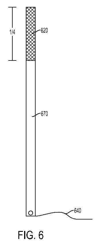
[0094] An example of an antenna partially coated with a conductive particle based antenna enhancer is described below with reference to FIG. 6.
[0095] FIG. 6 illustrates an antenna partially coated with a conductive particle based antenna enhancer according to an exemplary embodiment of the present invention. The particular structure of the antenna partially coated with the conductive particle based antenna enhancer shown in FIG. 6 is merely an example used for explanation and is not intended to be limiting. The conductive particle based material used to fabricate the conductive particle based antenna of FIG. 6 is assumed to be formulated as a liquid, paint, gel, ink, or paste that dries or cures.
[0096] Referring to FIG. 6, an antenna 670 that is connected to a feed line 640 is shown. The antenna 670 is partially coated with a conductive particle based antenna enhancer 620. As can be seen, the conductive particle based antenna enhancer 620 coats about a quarter of the antenna 670.
[0097] Tests were conducted to compare a conventional copper antenna to the conventional copper antenna with the conductive particle based antenna enhancer. In particular, the same equipment and testing conditions as the test described above with respect to the conductive particle based antenna were performed. Here, insulative tape was applied to the entirety of the conventional copper antenna and the conductive particle based material was then applied onto the insulative tape.
[0098] The test data for the conventional copper antenna and the conventional copper antenna that has been enhanced with the conductive particle based antenna enhancer are provided below in Table 2.
[0000]
TABLE 2
Conventional Copper Antenna with Conventional Conductive Particle Based Antenna Copper Antenna Enhancer
Forward Power 22 watts 28 watts
Reverse Power 12 watts 10 watts
Relative Signal -35 decibels -27 decibels
Strength
[0099] As can be seen in Table 2, the conventional copper antenna with the conductive particle based antenna enhancer exhibits a significantly higher forward power (i.e., 28 watts) than the forward power of the conventional copper antenna alone (i.e., 22 watts). This can be explained by the conventional copper antenna with the conductive particle based antenna enhancer exhibiting a significantly lower reverse power (i.e., 10 watts) than the reverse power of the conventional copper antenna alone (i.e., 12 watts). Accordingly, the resulting relative signal strength of the conventional copper antenna with the conductive particle based antenna enhancer is higher (-27 decibels) than the resulting relative signal strength of the conventional copper antenna (-35 decibels).
[0100] As can be gleaned from the above identified test, the conventional copper antenna with the conductive particle based antenna enhancer is more efficient at emitting electromagnetic signals into space than the conventional copper antenna alone. Therefore, the conventional copper antenna with the conductive particle based antenna enhancer has a higher effective gain than the conventional copper antenna alone. Also, since there is less reverse power, less of the electromagnetic radiation input to the conventional copper antenna with the conductive particle based antenna enhancer will be converted into heat. Thus, the conventional copper antenna with the conductive particle based antenna enhancer may operate at a lower temperature for a given input power and therefore may have a higher power rating.
[0101] Accordingly, the conductive particle based material may be used to enhance a conventional antenna.
Conductive Particle Based Transmission Line
[0102] The conductive particle based material may be used to form a conductive particle based transmission line. To implement a conductive particle based transmission line, a transmission line is formed in any of the various ways described herein for forming an object using the conductive particle based material. Herein, at least some of the properties that enable the conductive particle based material to efficiently radiate electromagnetic radiation into space allow the conductive particle based material to efficiently radiate electromagnetic radiation down the transmission line formed using the conductive particle based material. The use of the conductive particle based material as a transmission line is beneficial due to its lower resistance and heat generation.
Conductive Particle Based Electromagnetic Radiation Harvester
[0103] The conductive particle based material may be used as an electromagnetic radiation harvester. The high efficiencies of the conductive particle based material in at least one of propagating and absorbing electromagnetic radiation make it ideally suited for use in collecting electromagnetic radiation. While such collected electromagnetic radiation may be electromagnetic radiation that was transmitted with the intention of being harvested by the electromagnetic radiation harvester, the collected electromagnetic radiation may be background electromagnetic radiation. Herein, the electromagnetic radiation harvester may be coupled to a receiver that collects the energy absorbed by the electromagnetic radiation harvester. The electromagnetic radiation harvester is formed in any of the various ways described herein for forming an object using the conductive particle based material.
Conductive Particle Based Conformable Antenna
[0104] The conductive particle based material may be used to construct a conductive particle based conformable antenna. The benefit of the conductive particle based conformable antenna may be easily appreciated when considered in the context of an exemplary use case, which is described below.
[0105] According to the exemplary use case, the conductive particle based conformable antenna may use used in a military setting. The Special Operations community has a major logistical and safety issue when it comes to communications in the theater. The US Department of Defense (DoD) has rapidly expanded its communications capabilities within the radio spectrum. In the past, two way radios in a variety of form factors where used for conventional Push-To-Talk (PTT) communications. The use of these systems has now evolved into a true "Digital Battlefield" consisting of a multitude of communications platforms. Vast arrays of data networks came into reality. The scope of radios used today varies widely from conventional voice to Satellite, mesh networks, to Unmanned Aerial Vehicles (UAVs) and unattended ground sensors.
[0106] The reason this wide variety of systems is mentioned is to give an understanding of why the conductive particle based conformable antenna may be beneficial to the mission of soldiers. Every RF device utilized by the military operates on a wide range of frequencies and a different type of transmission (Amplitude Modulation (AM), Frequency Modulation (FM), Satcom, Single Side band, etc.).
[0107] However, conventional antenna systems are designed and tuned for a limited range of frequencies and are generally designed to work with only one of the hundreds of types of radio devices on the market. The other major downsides to these conventional antenna systems are the logistics of getting them into battle. They are heavy, bulky, expensive, and difficult to transport. Accordingly, there is a need to address the shortcomings of the conventional antenna systems.
[0108] The conductive particle based conformable antenna addresses the shortcomings of the conventional antenna systems by being operable with any and all of the radios currently deployed and being developed. As opposed to being an antenna of fixed form, the conductive particle based conformable antenna may instead be constructed on an as needed basis.
[0109] For example, the conductive particle based conformable antenna may be constructed on site using the conductive particle based material. In this case, the conductive particle based material is a liquid, paint, gel, ink or paste that dries or cures. Herein, the conductive particle based conformable antenna may be applied to a substrate. In particular, the conductive particle based material may be sprayed on, brushed on, rolled on, silk screened, ink jet printed, etc.
[0110] The conductive particle based conformable antenna may be designed based on typical antenna design, theory, and formulas. The antenna design may be generated in advance or at the time the antenna is needed based on desired characteristics.
[0111] The conductive particle based material is applied to the substrate to form the conductive particle based conformable antenna based on the desired antenna design.
[0112] The substrate may be any surface of any material, such as acrylic, ABS, structural foams, solvent sensitive materials such as polycarbonate and polystyrene, and non-porous surfaces including primed wallboard, wood and clean metals, etc.
[0113] When the substrate is a conducting material, a non-conductive or semi-conductive coating may first be applied to the substrate. In this case, the conducting material may serve as a ground plane. When the substrate is a non-conducting material, a ground plane can be accomplished by using the earth's natural ground. Alternatively, the ground plane can be accomplished by fabricating an independent ground plane.
[0114] Once the antenna is fabricated, a feed line is coupled to the conductive particle based conformable antenna and an RF communications device. The conductive particle based conformable antenna is at least one of electrically, capacitively, and inductively coupled to a coupling point of the feed line. The conductive particle based conformable antenna may be coupled to the coupling point of the feed line at an end point of the conductive particle based conformable antenna. When capacitively or inductively coupled, the coupling may occur through a distance that includes an air gap or a substance, such as glass.
[0115] To fabricate the conductive particle based conformable antenna, a template of the desired antenna design may be used. The template may be a sheet formed of any rigid or semi-rigid material in which the desired design of the antenna is cut out.
[0116] An example of a template used to fabricate a conductive particle based conformable antenna is described below with reference to FIG. 7.
[0117] FIG. 7 illustrates a template used to fabricate a conductive particle based conformable antenna according to an exemplary embodiment of the present invention.
[0118] Referring to FIG. 7, a template 700 is shown. The template 700 may be any material that may be used to form a template or stencil. For example, the template 700 may be a sheet formed of a rigid or semi-rigid material. The cut out of the template 700 may be at least one of a positive and a negative of a desired design of an antenna. The template 700 may be an image displayed on a surface showing where conductive particle based material should or should not be applied. The template 700 may be an image displayed on a display or in a guide book that shows a desired design of an antenna. Herein, the template 700 shown in FIG. 7 corresponds to the antenna design shown in FIG. 2.
[0119] Examples of various cutout designs for the template 700 are found in U.S. Design patent application Ser. No. 29/390,425, filed on Apr. 25, 2011, and entitled "ANTENNA"; U.S. Design patent application Ser. No. 29/390,427, filed on Apr. 25, 2011, and entitled "ANTENNA"; U.S. Design patent application Ser. No. 29/390,432, filed on Apr. 25, 2011, and entitled "ANTENNA"; U.S. Design patent application Ser. No. 29/390,435, filed on Apr. 25, 2011, and entitled "ANTENNA"; U.S. Design patent application Ser. No. 29/390,436, filed on Apr. 25, 2011, and entitled "ANTENNA"; U.S. Design patent application Ser. No. 29/390,438, filed on Apr. 25, 2011, and entitled "ANTENNA"; and U.S. Design patent application Ser. No. 29/390,442, filed on Apr. 25, 2011, and entitled "ANTENNA", the entire disclosure of each of which is hereby incorporated by reference.
[0120] An exemplary method for fabricating a conductive particle based conformable antenna using a template is described below with reference to FIG. 8.
[0121] FIG. 8 illustrates a method for fabricating a conductive particle based conformable antenna using a template according to an exemplary embodiment of the present invention. Herein, the conductive particle based material used to fabricate the conductive particle based conformable antenna is assumed to be formulated as a liquid, paint, gel, ink, or paste that dries or cures.
[0122] Referring to FIG. 8, a template and substrate is chosen in step 800. In step 810, the chosen template may be fixed against the chosen substrate. In step 820, the conductive particle based material may then be applied on the template such that the conductive particle based material passes through at least one cut out portion of the template so as to be applied to the corresponding portion of the substrate. The conductive particle based material may be applied until its particle density reaches a certain threshold. This may be determined by measuring the resistance of the material across the length of the antenna (or antenna segment). Here, the threshold may correspond to a predefined resistance or range of resistances (e.g., 11-15 ohms).
[0123] The template may then be removed leaving the conductive particle based material to dry or cure on the chosen substrate according to the desired design. In step 830, one or more coupling points of a feed line may be affixed to the conductive particle based conformable antenna. Herein, step 830 may be omitted. In addition, additional steps may be included, such as applying at least one of an insulative coating, a surface preparation coating, a protective coating, and a concealment coating. Any or all of this fabrication technique may be automated, as will be described below.
[0124] While a conductive particle based conformable antenna is described herein, any disclosure related to a conductive particle based conformable antenna is equally applicable to a conductive particle based conformable antenna enhancer.
Fabrication Techniques for Conductive Particle Based Conformable Antenna
[0125] In one exemplary embodiment, techniques for constructing a conductive particle based conformable antenna are described. Herein, a computerized device is used to generate a template that is used to construct a conductive particle based conformable antenna.
[0126] The computerized device may be any of a desktop computer, a laptop computer, a netbook, a tablet computer, a Personal Data Assistant (PDA), a Smartphone, a portable media device, a specialized mobile device, etc. The computerized device may include one or more of a display, an input unit, a control unit, a printer, memory, a communications unit, and a projection unit.
[0127] The conductive particle based conformable antenna that is constructed using the template may be formed using the conductive particle based material that is sprayable, rollable or brushable. The conductive particle based material may be applied directly onto any substrate. The conductive particle based conformable antenna, once fabricated onto a surface, may be painted over with a paint in order to conceal the antenna, provide protection to the antenna, or provide the antenna with desired aesthetics.
[0128] According to an exemplary embodiment of the present invention, to create and install an antenna, the computerized device may be used to generate the template. The computerized device may include a graphical user interface that queries a user regarding certain characteristics/criteria or otherwise allows a user to enter certain characteristics/criteria. Based on the input characteristics/criteria, the computerized device generates the template. Herein, the user may input less than all of the characteristics/criteria. In this case, the characteristics/criteria not input by the user may be obtained via a formula, or a local or remote database. In addition, assumed values for the characteristics/criteria not input by the user may be used.
[0129] Examples of the characteristics/criteria include one or more of a substrate on which the antenna will be disposed, frequency of operation, aperture or antenna pattern, whether a space saving design is desired, velocity factor, resonant frequency, Q factor, impedance, gain, polarization, efficiency, bandwidth, heat characteristics, type of amplifier, environment, etc. Further, one or more of the characteristics/criteria may include a number of preset options for a given characteristic/criteria. For example, the options for the substrate on which the antenna will be disposed may include one or more of wood, metal, glass, plastic, etc. For another example, the options for the desired antenna pattern include one or more of an omni-directional antenna pattern, a directional antenna pattern, a circular antenna pattern, a phased array antenna pattern, etc.
[0130] The computerized device may guide a user in inputting at least one of the one or more the characteristics/criteria and may request additional information from the user.
[0131] Based on the input one or more characteristics/criteria, the computerized device determines an antenna pattern using a pattern determination algorithm. The antenna pattern may be a preset antenna pattern or an antenna pattern formed based on an algorithm and the input one or more characteristics/criteria. In addition, the computerized device may determine one or more of a scaling factor of the antenna pattern, dimensions of the antenna pattern or elements of the antenna pattern, grain direction, application notes, etc. Alternatively, or additionally, the characteristics/criteria may not be preset.
[0132] The computerized device may determine more than one antenna pattern and may allow a user to select a desired antenna pattern from among the determined more than one antenna pattern.
[0133] Once the antenna pattern is determined, as well as one or more of the scaling factor of the antenna pattern, dimensions of the antenna pattern or elements of the antenna pattern, grain direction, application notes, etc., a resulting template may be at least one of displayed on the display of the computerized device, projected onto a surface using the projection unit of the computerized device, and printed using one of an external and an integrated printed. When a projection unit is employed, the computerized device may further include a device that adjusts the scale of the projected template based on at least the distance between the projection unit and the surface on which the antenna is to be constructed. Further, when a projection unit is employed, the computerized device may further include a device that adjusts the location of the projected template so that the projected template remains on the same location of the surface regardless of the movement of the computerized device. The template may then be used to construct the antenna.
[0134] Also, the template may correspond to digital data that is stored in a storage device or communicated to another device that applies the antenna material based on the digital data.
[0135] In one exemplary embodiment, the computerized device communicates the input characteristics/criteria to a remote computerized device which determines one or more of the antenna pattern, the scaling factor of the antenna pattern, dimensions of the antenna pattern or elements of the antenna pattern, grain direction, application notes, etc., which is then communicated to the computerized device.
[0136] In one exemplary embodiment, the antenna patterns may be stored remotely from the computerized device and communicated to the computerized device before or after the antenna pattern is determined. The antenna patterns may be communicated to the computerized device in response to a request by the computerized device or another entity.
[0137] An exemplary method for fabricating a conductive particle based conformable antenna using a computerized device is described below with reference to FIG. 9.
[0138] FIG. 9 illustrates a method for fabricating a conductive particle based conformable antenna using a computerized device according to an exemplary embodiment of the present invention.
[0139] Referring to FIG. 9, in step 900, the characteristics/criteria are obtained by the computerized device as described above. In step 910, an antenna pattern is selected by the computerized device based on the obtained characteristics/criteria, as described above. In step 920, a template is generated as described above.
[0140] An example of the computerized device described above is described below with reference to FIG. 10.
[0141] FIG. 10 illustrates a structure of computerized device used for fabricating a conductive particle based conformable antenna according to an exemplary embodiment of the present invention.
[0142] Referring to FIG. 10, the computerized device includes a controller 1010, a display unit 1020, a memory unit 1030, an input unit 1040, a communications unit 1050, a template generator 1060, and an antenna generator 1070. One or more of the components of the computerized device shown in FIG. 10 may be omitted. Also, the functions of one or more of the components of the computerized device shown in FIG. 10 may be performed by a combined component. In addition, additional components may be included with the computerized device.
[0143] The controller 1010 controls the overall operations of the computerized device. More specifically, the controller 1010 controls and/or communicates with the display unit 1020, the memory unit 1030, the input unit 1040, the communications unit 1050, the template generator 1060, and the antenna generator 1070. The controller 1010 executes code to have performed or perform any of the functions/operations/algorithms/roles explicitly or implicitly described herein as being performed by a computerized device. The term "code" may be used herein to represent one or more of executable instructions, operand data, configuration parameters, and other information stored in the memory unit 1030.
[0144] The display unit 1020 is used to display information to a user. The display unit 1020 may be any type of display unit. The display unit 1020 may be integrated with or separate from the computerized device. The display unit 1020 may be integrated with the input unit 1040 to form a touch screen display. The display unit 1020 performs any of the functions/operations/roles explicitly or implicitly described herein as being performed by a display.
[0145] The memory unit 1030 may store code that is processed by the controller 1010 to execute any of the functions/operations/algorithms/roles explicitly or implicitly described herein as being performed by a computerized device. In addition, one or more of other executable instructions, operand data, configuration parameters, and other information may be stored in the memory unit 1030. Depending on the exact configuration of the computerized device, the memory unit 1030 may be volatile memory (such as Random Access Memory (RAM)), non-volatile memory (e.g., Read Only Memory (ROM), flash memory, etc.) or some combination thereof.
[0146] The input unit 1040 is used to enable a user to input information. The input unit 1020 may be any type or combination of input unit, such as a touch screen, keypad, mouse, voice recognition, etc.
[0147] The communications unit 1050 transmits and receives data between one or more entities. The communications unit 1050 may include any number of transceivers, receivers, and transmitters of any number of types, such as wired, wireless, etc.
[0148] The template generator 1060 may perform any of the functions/operations/algorithms/roles explicitly or implicitly described herein as being performed when generating a template. For example, the template generator 1060 may be a printer, a cutter, a projector, a display, etc.
[0149] The antenna generator 1070 may perform any of the functions/operations/algorithms/roles explicitly or implicitly described herein as being performed when generating an antenna. For example, the template generator 1060 may be a sprayer that sprays the conductive particle based material onto a substrate.
[0150] Herein, the functionality described above of the computerized device may result from an application installed on and being executed by the computerized device.
[0151] At this point it should be noted that the present exemplary embodiment as described above typically involve the processing of input data and the generation of output data to some extent. This input data processing and output data generation may be implemented in hardware, or software in combination with hardware. For example, specific electronic components may be employed in a mobile device or similar or related circuitry for implementing the functions associated with the exemplary embodiments of the present invention as described above. Alternatively, one or more processors operating in accordance with stored instructions (i.e., code) may implement the functions associated with the exemplary embodiments of the present invention as described above. If such is the case, it is within the scope of the present disclosure that such instructions may be stored on one or more non-transitory processor readable mediums. Examples of the non-transitory processor readable mediums include ROM, RAM, Compact Disc (CD)-ROMs, magnetic tapes, floppy disks, and optical data storage devices. The non-transitory processor readable mediums can also be distributed over network coupled computer systems so that the instructions are stored and executed in a distributed fashion. Also, functional computer programs, instructions, and instruction segments for accomplishing the present invention can be easily construed by programmers skilled in the art to which the present invention pertains.
[0152] While the invention has been shown and described with reference to certain exemplary embodiments thereof, it will be understood by those skilled in the art that various changes in form and details may be made therein without departing from the spirit and scope of the invention as defined by the appended claims and their equivalents.
ChamTech
Patents
Antenna
USD652029
Antenna
USD652410
Antenna
USD652028
Antenna
USD652027
Antenna
USD652409
NEAR FIELD COMMUNICATIONS SYSTEM HAVING ENHANCED SECURITY
WO2009021220
SYSTEM AND METHOD FOR NEAR FIELD COMMUNICATIONS HAVING LOCAL SECURITY
WO2009042977
Nano
Copper
NANO-COPPER PATENTS
Surface plasmon resonance rectenna and preparation method therefor
CN102544182
The invention provides a surface plasmon resonance rectenna and a preparation method therefor. The surface plasma resonance rectenna adopts a three-layer structure, wherein the lower layer is made from metal Ti; a TiO2 nanotube array layer is generated on one surface of the metal Ti in an oxidation manner; a Cu nano particle metal layer is arranged on the surface of the TiO2 nanotube array layer through photodeposition; and the micro-surface appearance of the Cu nano particle metal layer is nano particles. In the invention, as photodeposition replaces ultrahigh vacuum electron beam evaporation technology, and inexpensive metal copper Cu replaces precious metal Au to prepare the rectenna adopting the Ti/TiO2NT/Cu structure, the difficult problem that the conventional metal layer can not be used in large-scale industrial production due to high cost in deposition technology, equipment investment and precious metal, and green low-cost development of solar energy technology is facilitated.
Method for preparing copper nanowires and copper nano pointed cones
CN102776469
The invention discloses a method for preparing copper nanowires and copper nano pointed cones. The method comprises the steps of heating a copper substrate in oxygenated atmosphere to form a copper oxide thin film or a copper oxide nanowire thin film, placing the films into a vacuum chamber, performing bombarding by using a argon ion source, and controlling the energy and the time of the ion bombarding to obtain nanowires or copper nano pointed cone arrays. According to the method, no catalyst is used, copper nanowires and copper nano pointed cones, which have different density and sizes are prepared on the substrate conveniently, and the prepared copper nanowires and copper nano pointed arrays can be applied to photoelectric devices such as a display device, a lithium battery, a super capacitor and the like.
Method for preparing ultrafine copper powder for electronic paste
CN102764898
The invention belongs to the field of electronic paste and particularly relates to a method for preparing a ultrafine copper powder for the electronic paste, comprising the step of adding a dispersing agent and a reducing agent into a copper salt aqueous solution to reduce the elemental copper. The method is characterized in that nano-copper particles are added into the copper salt aqueous solution before the dispersing agent and the reducing agent are added, wherein the nano-copper particles have the size of 5-20nm, and the addition amount of the nano-copper particles is 0.3-0.6 per mill of the mass of copper salt in the copper salt aqueous solution. The method is simple in process and flexible to operate. The raw materials are nontoxic, environmentally friendly and suitable for industrial production. The ultrafine copper powder prepared by the adopting the method has uniform and controllable particle size, a narrow distribution range and high purity.
Preparation method of nano porous copper capable of being patterned
CN102766893
The invention discloses a preparation method of nano porous copper capable of being patterned, comprising the following steps: (1), sputtering a Cr-Cu seed layer on a sheet glass, spin coating positive photo-resist, baking the photo-resist, exposing, and developing in turn, so as to pattern the nano porous copper photo-resist; (2), depositing a copper stress buffer layer and a Cu-Zn alloy layer by the electro-deposition technique, to obtain a patterned precursor alloy thin film; and (3), performing de-alloying treatment on the patterned Cu-Zn patterned precursor alloy thin film in an acidic solution, removing the positive photo-resist, finally implementing the patterned nano porous copper so as to obtain a nano porous copper array. The preparation method and the micro-processing technique are compatible; specifically, the nano porous copper arrays with various patterns are obtained by the photo resist patterning technique, the Cu-Zn alloy co-deposition technique, and the de-alloying technique; the preparation method has the advantages of simple process, low cost, easy control, and good compatibility to the micro-processing technique.
Method for preparing nano copper lubricating material by wire electrical explosion method
CN102744414
The invention relates to a method for preparing a nano copper lubricating material by a wire electrical explosion method. On the aspect of preparing the nano lubricating material, the method effectively solves the agglomeration problem in the process of preparing nano metal powder by the existing electrical explosion method and fundamentally eliminates the problems of derivatives and impurities in the process of preparing the nano lubricating material by a chemical method. The method comprises the specific steps of: by a device comprising parts such as a high voltage discharge system, a wire throwing system, a liquid circulating system, a vacuum system, an explosion chamber and the like, after vacuumizing to the pressure of minus 0.1MPa and filling argon to the pressure of 0.1 to 0.2MPa, implementing effective crushing on a copper wire section with the specification of phi 0.2*(35 to 60)mm under a voltage of 7 to 13KV and simultaneously infiltrating the obtained product into lubricating oil; and in the electrical exploding process, directly generating a modified thin film on the surface of nano copper powder so as to form nano lubricating oil.
NANOMETER-SIZED COPPER-BASED CATALYST, PRODUCTION METHOD THEREOF, AND ALCOHOL PRODUCTION METHOD USING THE SAME THROUGH DIRECT HYDROGENATION OF CARBOXYLIC ACID
EP2561928
Also published as: US2013030224 (A1) WO2011132957 (A2) WO2011132957 (A9) WO2011132957 (A3) CN102946994 (A)
Disclosed is a nano-sized Cu based catalyst and a method of preparing the same including dissolving, in an aqueous solution, a first component comprising a Cu precursor, a second component precursor comprising one or more selected from the group consisting of a transition metal, an alkaline earth metal and a Group IIIb metal, and a third component precursor comprising one or more selected from the group consisting of alumina, silica, silica-alumina, magnesia, titania, zirconia and carbon and then performing stirring; precipitating the stirred mixture solution using Na2CO3 and NaOH to form a catalyst precursor precipitate; and washing and filtering the formed catalyst precursor precipitate. Also a method of preparing alcohol is provided, including reacting hydrogen with carboxylic acid including a single acid or an acid mixture of two or more acids derived from a microorganism fermented solution, using the nano-sized Cu based catalyst.
Copper nano powder and preparation method of copper nano powder
CN102601381
The invention discloses copper nano powder and a preparation method of the copper nano powder. The powder is prepared by the following methods: preparing copper salt solution from copper salt, adding a drag reduction agent and an inhibitor into the copper salt solution to prepare copper salt mixing solution and pre-heating the copper salt mixing solution; preparing reducing agent solution, adjusting the pH value of the reducing agent solution, and pre-heating the reducing agent solution; uniformly mixing and agitating the copper salt mixing solution and the reducing agent solution, heating the mixture to the reaction temperature to enable the mixture to react for a certain time so as to obtain nano copper suspension solution; aging the nano copper suspension solution; performing vacuum filtration on the suspension solution obtained from the above steps to obtain the copper nano powder in which the impurity is not removed; processing the copper nano powder to obtain the copper nano powder cladded by organic solvent; performing vacuum filtration on the copper nano powder to obtain wet copper nano powder, and performing low-temperature vacuum drying on the copper nano powder obtained from the above steps so as to obtain the copper nano powder product. The powder is small in particle size and narrow in particle size distribution. The method is controllable in reaction process, simple in technology and suitable for industrial production.
Water-soluble nano-copper and preparation method thereof
CN102554217
The invention belongs to the technical field of nanometer materials, and particularly relates to water-soluble nano-copper and a preparation method of the water-soluble nano-copper, wherein the water-soluble nano-copper is nano-copper clusters which are surface-modified by stable organic single molecules formed in a way that organic compound surface modifier containing sulfydryl is bonded on the surface of copper nanoparticles. The invention can obtain copper nanoparticles which can be effectively dispersed in water phases and can exist stably, and is simple in preparation process and preparation devices, low in raw material cost, low in the production cost, high in yield, and suitable for large-scale industrial production, and the raw materials are easily accessible.
New method of preparing powder nano material
CN1436626
The new nano powder material preparing process of the present invention is suitable for preparing carbide, nitride and particle metal powder. The preparing process includes pumping the reactor into vacuum, filling protecting gas or reaction gas, setting graphite electrode inside the reactor, applying voltage between the graphite electrode and the metal inside the crucible inside the reactor to produce high temperature carbon arc and metal vapor. When protecting gas is filled, nano nickel powder, copper powder, aluminum powder and other metal powder coated by graphite atoms with less agglomeration may be prepared. When reaction gas is filled, nano carbide or nitride powder may be prepared. Compared with available technology, the produced nano powder has less agglomeration, the production process has low cost and great arc power and is suitable for large scale production and is widely applicable.
METHOD FOR PREPARING NANO-PARTICLES
EP1550633
Also published as: EP1550633 (A4) EP1550633 (B1) US2004197884 (A1) US7204999 (B2) JP3703479 (B2) more
The method of the production of a nanoparticle of the present invention includes a step of forming a nanoparticle including a compound of a metal ion in a cavity part of a protein, in a solution containing the protein having the cavity part therein, the metal ion, and a carbonate ion and/or a hydrogen carbonate ion. Examples of the aforementioned compound include e.g., a hydroxide. The aforementioned metal ion is preferably any one of a nickel ion (Ni<2+>), a chromium ion (Cr<2+>) or a copper ion (Cu<2+>). According to the aforementioned method, nanoparticles having a uniform particle diameter can be produced.
Method for manufacturing nano-copper
CN1557589
The present invention is nano copper preparing process and belongs to the field of nano material preparing technology in radiochemistry. The technological process includes adopting copper sulfate as copper source, isopropanol as oxidant clearer in water solution, hydrophilic suitable for PVA for controlling the crystal kernel growth speed and grain size and electronic accelerator to produce electron beam for irradiation treatment; washing irradiated solution, centrifugal separation and stoving to obtain claret nano copper powder. The present invention has simple technological process, short production period, no pollution and high safety.
Method for preparing nano copper particle
CN1709617
Also published as: US2006053972 // US7422620
The invention discloses a method for preparation of nm copper grains with very perfect dispersitivity. It comprises copper hydrosol prepared by reduction method, using organic liquor which contains specifical extraction solution to extract copper colloidal granules, and altering polarity of the organic phase to separate nm copper granules. The preparation has very many characteristics, for example, cheap and handy raw material, simplicity and convenience, low cost, high productivity and so on. It fits large-scale industrial production and the diameter of manufactured nm copper granules is between one and ten nm. Also it stabilizes in the air and is able to scatter in the industrial non-polarity organic liquor and kinds of lube. In conclusion, it has extensive industrial purposes.
POWDERS OF NANO CRYSTALLINE COPPER METAL AND NANO CRYSTALLINE COPPER ALLOY...
WO2005092541
A nano crystalline copper metal powder, which comprises aggregates of nano crystal grains of copper metal or a copper alloy, wherein the nano crystal grain has a size of 2 to 1000 nm; a bulk material of a nano crystal copper or copper alloy exhibiting high hardness, high strength, high electric conductivity and high toughness, which comprises a great number of above nano crystal grains being firmly bound with one another; and a method for producing the above bulk material of a nano crystal copper or copper alloy exhibiting high hardness, high strength, high electric conductivity and high toughness, which comprises subjecting the above copper powder or copper alloy powder to a solidification forming such as a vacuum hot solidification forming or an explosive forming, for example, a spark plasma sintering at a temperature of 250 to 700 DEG C, hot pressing, sheath rolling, hot forging, extruding or hot isotropic pressure forming (HIP).
A method and apparatus for the production of copper nanofluids by using chemical method
TWI262111
A method for the production of copper nanofluids uses chemical reduction method. For synthesis of nanofluids containing Cu nanoparticles, copper precursor and reactants (e.g. reducing agent) are mixed uniformly. By controlling the reaction rate and environment, copper particle in nano scale is obtained through nucleation and growth process. The copper nanoparticle can increase the thermal conductivity of nanofluids with its higher thermal conductivity compared with that of fluids.
Preparation of nano copper fluid
CN101264525
The invention relates to a preparation process, belonging to the technical field of the preparation processes for inorganic materials, which comprises the following steps: metallic copper salt and polyethylene pyrrolidone are dissolved into ethylene glycol to form settled solution, then reducing agent is added into the solution and mixed evenly; the mixed liquor is put into a microwave stove for heating and reaction, after cooling, Cu/ ethylene glycol nanometer fluid is obtained. Therefore, the preparation process has the advantages of simple process, low cost, high yield, and facility for industrial production; moreover, the product acquired by use of the preparation process has the advantages of good dispersibility, long-term stability with a plurality of better performances than prior products, and wide popularization and application prospects.
Production of nano-catalyst
CN101028600
A process for preparing the nano-catalyst used to selectively adsorb and convert harmful substances includes such steps as adding copper sulfate and manganese sulfate to deionized water, heating to 80-90 deg.C, stirring, adding strong alkali solution, stirring, filtering, washing the filtered cake until it becomes neutral, drying, calcining, cooling and sieving.
ELECTRODE, AND APPARATUS AND METHOD FOR MANUFACTURING METALLIC FINE PARTICLE
JP2007270184
PROBLEM TO BE SOLVED: To provide a method for manufacturing copper nano particles by which granular nano sized metal fine particles are efficiently manufactured without growing a reduced metal like dendrite (tree branch) and without enlarging the particle size in the mass production of the particles. ; SOLUTION: In the method of manufacturing the copper nano particles, the copper nano particles are manufactured by applying current between an anode comprising copper and a cathode comprising aggregate of many acicular projections of platinum and electrically insulated from the anode. The platinum acicular projections are, for example, cylindrical platinum having <=1 [mu]m diameter or rectangular platinum having <=1 [mu]m one side length and electrolytically deposited on a conductive electrode.
Method for preparing nano copper powder and copper slurry
CN101077529
The present invention is process of preparing nanometer copper powder and copper slurry with high antioxidant performance. The process includes solvent replacement, the first reduction, the second reduction, separation, drying and other steps. The present invention has the features of simple preparation process at normal temperature and normal pressure, low production cost, the effective protection of produced nanometer copper particle in organic phase, small copper powder size, environment friendly preparation process, etc. The prepared nanometer copper powder and copper slurry may be applied in producing large scale PCB, conducting ink, multilayer ceramic capacitor, etc.
Method for preparing nano copper powder
CN101372037
The invention discloses a method for preparing copper nanoparticle. The preparation method is as follows: cupric salt is taken as raw materials; hydroborate serves as reducer; reducer aqueous solution is poured into cupric salt aqueous solution which complexes with ammonia and is stirred quickly, when the cupric salt aqueous solution becomes colorless, the copper nanoparticle is prepared. When the stirring is stopped, the copper nanoparticle sinks quickly, the supernatant fluid is dumped. The copper nanoparticle is washed with water repeatedly, stands and is clarified, and the supernatant fluid is dumped. Finally being filtered, the copper nanoparticle with good dispersibility is prepared by being dried in the flow argon atmosphere. The preparation method has simple production technology, is easy to operate. The copper nanoparticle can be produced on a large scale; and an appropriate covering layer can be covered on the surface of the copper nanoparticle.
COPPER MICROPARTICLE, METHOD FOR PRODUCTION OF COPPER MICROPARTICLE
WO2008041780
Disclosed is a method for producing a copper microparticle, which comprises: a first reduction step for mixing an unsaturated fatty acid solution containing a copper ion with an aldose (a reducing monosaccharide) solution to form an emulsion; a second reduction step for adding an aqueous ascorbic acid solution to the emulsion; and a copper microparticle separation step. The method can produce a copper microparticle which has an average particle diameter of 100 nm or smaller and whose surface is partly or entirely modified with a carboxyl terminal group derived from the unsaturated fatty acid. The copper microparticle produced by the methodshows high dispersibility in spite of having a nano-order size.
METHOD FOR MANUFACTURING METAL NANO PARTICLE SOLUTION
US2009176875
A method for manufacturing a stabilized metal nano particle solution is disclosed. This method manufactures a metal nano particle solution so as to make a metal substance such as silver, gold, copper, zinc or cobalt into ultra-capsular nano particles. That is to say, this new method is simple and suitable for mass production without requiring any separate reducer putting process at a room temperature while a transition metal nano particle solution is produced. In this method, an alcohol solution including a metal salt solution and a soluble polymer is mixed at a room temperature to make a nano metal particle solution with a particle size of 100 nm or less.
Method for preparing metallic simple substance nano-crystal material
CN101279374
A method for preparing metal single substance nanocrystalline materials is applicable to the preparation of the metal nanocrystalline materials of copper, silver, lead, palladium, tin, antimony and so on. A melted composite alkali metal hydroxide solvent is used for carrying out the chemical reaction synthesis under the atmospheric pressure and the temperature of 100 to 300 DEG C, the used raw materials are soluble inorganic metal salts and zinc powder or iron powder, the cost during the synthesis process is low, various parameters in the reaction process are easy to be monitored and controlled, the environmental pollution is less, the evenness of a reaction system is good, the process is simple and the production is easy to be enlarged; ; furthermore, the obtained metal crystal has good crystallization, clean surface and even size, which is applicable to the research of intrinsic properties and the maximization of the functions of the nanocrystalline materials. The metal single substance nanocrystalline materials of the metal nanocrystalline materials are characterized by metal properties, electric and electronic properties, magnetic properties, chemical properties, thermal properties and luminous properties etc., which can be widely used in superconductive, chemical, medical, optical, electronic, electric appliance and other industries.
Surface finish nano copper/copper alloy particles and preparation thereof
CN101259531
The invention relates to a nano-copper/copper alloy particle for surface modification, which is prepared by the following method that: water solution of copper salt or copper salt and alloy component salt with the concentration of 0.001 to 1 mol/L is prepared, then the water solution is fully mixed with the mixed solution of a reductant, a surface modifier and a weak polar or non-polar organic solvent, the still placement is carried out for 30 to 180min after the reaction for 30 to 180min under the alkaline environment with pH of 8 to 13, the organic phase is obtained by separation, and the nano-copper/copper alloy particle for surface modification is obtained after the concentration.; The copper/copper alloy nanoparticle for surface modification which is provided by the invention has controllable particle size and distribution, difficult clustering, good antioxidant property, monodisperse property and good dispersion stability in the organic solvent. The preparation process and a device of the nano-copper/copper alloy particle for surface modification are simple, the raw materials are cheap and easy to obtain, the cost is low, and the yield is high, thus being applicable to the large-scale industrial production.
Method for preparing metallic copper nano particle
CN101337277
The invention relates to a method for preparing metallic copper nanoparticles, and belongs to the technical field of preparing nanomaterial by liquid-phase chemical reduction. The method adopts sodium hydrosulfite as a reducer to reduce cupric hydroxide under alkaline conditions, and adopts sodium dodecyl sulfate as a dispersant to generate copper nanoparticles with the grain diameter of 30 to 90nm. The method has the characteristics of simple technological process, low production cost and suitability for industrialized production.
Preparation method of whole continuous nano-porous copper
CN101596598
The invention relates to a preparation method of whole continuous nano-porous copper, comprising the following steps: (1) heating the pure metallic aluminum and copper to the molten state, stirring and mixing the mixture to form Cu-Al alloy liquid; (2) fast blowing the alloy liquid out with inert gas to solidify the molten liquid metal on the copper rollers which rotate in high speed and prepare alloy strips, or solidify the molten liquid metal in copper molds to prepare alloy plates or alloy bars; and (3) performing dealloying process to the obtained alloy, cleaning the alloy in the distilled water to be neutral and airing the alloy to obtain nano-porous copper. The beneficial effects of the invention are as follows: (1) the produced nano-porous copper is whole continuous and whole continuous nanosize bulk materials can also be prepared; (2) low concentration of corrosion solution is used to prepare nano-porous copper in the method of the invention, and the operation process is simple and the method is suitable for large-scale industrialized production; and (3) according to the components of the mother alloy and the types of corrosion solution, the structure and size of nanoporous copper can be regulated.
Preparation method of nano-copper
CN101607317
The invention belongs to the nanometer material technical field, in particular to a preparation method of nano-copper, comprising the following steps: dissolving copper salt and organic protective agents in a solvent, heating the solution to 30-100 DEG C, simultaneously adding reducing agent in the reaction system to react while stirring for 20-30min, then cooling gradually; standing the cooled solution, and then centrifuging and finally washing the solution with ethanol and acetone repeatedly to obtain pure nano-copper. The invention has simple process, mild reaction conditions and short reaction time; in the reaction process, two protective agents are both adopted to prevent the growth and oxidation of nano-copper; the product performance is good, the particle size of nano-copper is less than 20nm, the nano-copper can not be oxidized for one month in the air; the production cost is low and no hazardous waste can be generated, thus meeting the demand of 'green production'.
PROCEDURE FOR PRODUCTION OF NANO DISPERSED COPPER POWDER
RU2009147519
FIELD: metallurgy. ^ SUBSTANCE: procedure for production of nano dispersed copper powder by reduction consists in mixing copper salt with solution of glucose, in dissolving salt at heating, in introduction of sodium hydroxide, in conditioning under isothermal mode and in successive extraction of metal copper in form of nano dispersed powder. Also, sulphate of copper is used as copper salt. Copper sulphate is mixed with solution of glucose at mole ratio of glucose to copper equal to (1.0-2.5):1.0. Dissolving is carried out at 50-60C. Sodium hydroxide is introduced upon complete copper sulphate dissolving and solution heating to temperature 70C.; It is carried out gradually at several stages for maintaining pH equal to 6-11 in process of reduction reaction, preferably, to 8-9, first to formation of oxide of univalent copper, and further to metal copper. ^ EFFECT: simplified, with reduced prime cost process of production of nano dimension particles of copper due to reduced number of process operations of synthesis.
Method for preparing copper zinc tin sulfur selenium nano particles
CN101830444
The invention relates to a method for preparing copper zinc tin sulfur selenium nano particles, which belongs to the technical field of photoelectric materials. The method comprises the following steps of: 1, mixing divalent zinc salt, divalent tin salt and monovalent or divalent copper salt, adding surfactant into the mixture, and heating the mixture; 2, mixing sulfur powder with selenium powder, adding the surfactant into the mixture, and heating the mixture; and 3, injecting solution obtained by the step 2 into solution obtained by the step 1 for warming, and purifying a product to prepare the copper zinc tin sulfur selenium nano particles. The preparation method has the advantages of no pollution, mild and simple reaction condition and low cost, and is suitable for large-scale production. The forbidden band width of the copper zinc tin sulfur selenium nano particles can change with the proportion change of sulfur selenium.
Method for preparing flaky nano copper powder
CN101890504
The invention discloses a method for preparing flaky nano copper powder, comprising the following steps: compounding a copper salt aqueous solution with a surfactant to obtain a mixed solution A, wherein the water in the copper salt aqueous solution and the surfactant form a surfactant compound system; (2) compounding a reducing agent aqueous solution with the surfactant which is the same as that used in step (1) to obtain a mixed solution B, wherein the water in the reducing agent aqueous solution and the surfactant form the surfactant compound system; (3) mixing the mixed solution B obtained in step (2) and the mixed solution A obtained in step (1) by stirring at the temperature of 20 DEG C to 80 DEG C, and reacting completely with stirring; and (4) carrying out solid and liquid separation on the product, washing the solid, and carrying out vacuum drying to obtain the flaky nano copper powder. The method of the invention has mild condition, simple process, short production period, low equipment investment and low preparation cost, and is easy to realize industrial production. The prepared flaky nano copper powder has consistent appearance, uniform size and good dispersibility.
Method for preparing nano-copper
CN101890506
The invention relates to a method for preparing nano-copper. The method comprises the following steps of: dispersing a copper precursor into the liquid paraffin serving as a solvent and a reducing agent; adding a surfactant into the liquid paraffin with stirring; performing heat treatment for 2 to 4 hours in an atmosphere of N2 protective gas or no protective gas; standing; centrifuging to obtain a product; and alternately washing the product by using petroleum ether, distilled water or absolute ethyl alcohol to obtain the nano-copper. The nano-copper powder prepared by using the method has the advantages of particle sizes of less than 50 nm, uniform distribution, difficult oxidation, high dispersibility in polar solvents or non-polar solvents, cheap raw materials, low energy consumption, simple process equipment and easy large-scale production.
Preparation method of nano-copper powder
CN102586800
The invention discloses a preparation method of nano-copper powder, which comprises the following steps of: in a self-made special electrolytic cell, taking metal copper as an anode, taking conducting material as a cathode, taking electrolyte as organic alcohol, taking ammonium salt which is soluble in the electrolyte as electrolyte, forbidding the ammonium salt to participate chemical reaction, and combining the cathode copper with the organic alcohol, so that the precursor of the nano-copper can be generated; mixing the precursor of the nano-copper, the organic alcohol or the other saturated hydrocarbon with the unsaturated hydrocarbon liquid, and sealing the precursor of the mixed nano-copper in a high-pressure kettle to be subjected to reductive treatment, so that the nano-copper powder can be obtained; and separating the nano-copper powder from the mixture of the reduced nano-copper powder and the organic solvent by an industrial centrifugal machine device, and washing with industrial alcohol, so that wet nano-copper powder can be obtained, putting the nano-copper powder into a vacuum drying oven, and treating, so that the nano-copper powder which accords with the national standard can be obtained. The preparation method has the advantages of being free of pollution in reaction process, small in investment, low in cost, good in product dispersibility, even in distribution, and capable of realizing different-quantity production.
Water-soluble nano-copper and preparation method thereof
CN102554217
The invention belongs to the technical field of nanometer materials, and particularly relates to water-soluble nano-copper and a preparation method of the water-soluble nano-copper, wherein the water-soluble nano-copper is nano-copper clusters which are surface-modified by stable organic single molecules formed in a way that organic compound surface modifier containing sulfydryl is bonded on the surface of copper nanoparticles. The invention can obtain copper nanoparticles which can be effectively dispersed in water phases and can exist stably, and is simple in preparation process and preparation devices, low in raw material cost, low in the production cost, high in yield, and suitable for large-scale industrial production, and the raw materials are easily accessible.
Copper nano powder and preparation method of copper nano powder
CN102601381
The invention discloses copper nano powder and a preparation method of the copper nano powder. The powder is prepared by the following methods: preparing copper salt solution from copper salt, adding a drag reduction agent and an inhibitor into the copper salt solution to prepare copper salt mixing solution and pre-heating the copper salt mixing solution; preparing reducing agent solution, adjusting the pH value of the reducing agent solution, and pre-heating the reducing agent solution; uniformly mixing and agitating the copper salt mixing solution and the reducing agent solution, heating the mixture to the reaction temperature to enable the mixture to react for a certain time so as to obtain nano copper suspension solution; aging the nano copper suspension solution; performing vacuum filtration on the suspension solution obtained from the above steps to obtain the copper nano powder in which the impurity is not removed; processing the copper nano powder to obtain the copper nano powder cladded by organic solvent; performing vacuum filtration on the copper nano powder to obtain wet copper nano powder, and performing low-temperature vacuum drying on the copper nano powder obtained from the above steps so as to obtain the copper nano powder product. The powder is small in particle size and narrow in particle size distribution. The method is controllable in reaction process, simple in technology and suitable for industrial production.
Method for preparing single copper with porous micro/nano hierarchical structure
CN102672198
The invention discloses a method for preparing single copper with a porous micro/nano hierarchical structure. The method comprises the following steps of adding phenol and vitamin C into a mixed culture of copper ion and ammonia water under the condition of one atmosphere at the temperature of 10 to 30 DEG C; quickly reacting; and preparing the single copper with the porous micro/nano hierarchical structure. By adoption of the preparation method, special equipment and reaction conditions are not required, and heating and calcination are not required, or a porous matrix serving as a template is not required to be added. The method has the characteristics that the process is simple, the energy consumption is low, the yield is high and the like, and is environment-friendly and suitable for large-scale industrial production.
Method for preparing ultrafine copper powder for electronic paste
CN102764898
The invention belongs to the field of electronic paste and particularly relates to a method for preparing a ultrafine copper powder for the electronic paste, comprising the step of adding a dispersing agent and a reducing agent into a copper salt aqueous solution to reduce the elemental copper. The method is characterized in that nano-copper particles are added into the copper salt aqueous solution before the dispersing agent and the reducing agent are added, wherein the nano-copper particles have the size of 5-20nm, and the addition amount of the nano-copper particles is 0.3-0.6 per mill of the mass of copper salt in the copper salt aqueous solution. The method is simple in process and flexible to operate. The raw materials are nontoxic, environmentally friendly and suitable for industrial production. The ultrafine copper powder prepared by the adopting the method has uniform and controllable particle size, a narrow distribution range and high purity.
Nano Antennas
RADAR ANTENNA
WO9214277
SENSORS BASED ON NANO-STRUCTURED COMPOSITE FILMS
CA2105869
ANTENNA
JP7221533
Magnetic core element for antenna, thin-film antenna, and card equipped with thin-film antenna
US5567537
PHASED ARRAY ANTENNA
JP11127020
GPS RECEPTION SECTION GRAVITY CENTER REGULATOR (NANOBALANCER)
JP2000174534
ANTENNA AND COMMUNICATION DEVICE
JP2003298338
MAGNETIC COMPOSITE MATERIAL FOR ANTENNA TAG
JP2004179270
SMALL-SIZED HIGH-SENSITIVITY ANTENNA
JP2005057444
Antenna for shielding electromagnetic radiation emission
TWI241739
APPLICATIONS OF NANO-ENABLED LARGE AREA MACROELECTRONIC SUBSTRATES INCORPORATING NANOWIRES AND NANOWIRE COMPOSITES
WO2004032191
DEVICE FOR MANUFACTURING CARBON NANO-CAPSULE ENCAPSULATING DNA, METHOD FOR MANUFACTURING CARBON NANO-CAPSULE ENCAPSULATING DNA, AND CARBON NANO-CAPSULE ENCAPSULATING DNA
JP2005230970
Selective production of light-emitting ruthenium(II) ligand and mixed ligand complexes, used e.g. as molecular or nano-sensor, switch or wire, antenna, dendrimer, energy converter or photocatalyst, uses solvent and microwaves in first stage
DE102004009551
NANO-ANTENNA APPARATUS AND METHOD
WO2005119838
Ultra wide band signal receiver for ultra wide band data transmission system, has two sampling cell sets to sample waveform of signal received with preset delay, and correlator delivering detected signal
FR2881588
NANO STRUCTURE, MAGNETIC STORAGE MATERIAL USING IT, WIRING BOARD AND ANTENNA BASE MATERIAL
JP2006247795
Composition For Coating Organic Electrode And Method Of Manufacturing Organic Electrode Having Excellent Transparency Using The Composition
US2007200099
Microwave non reciprocal effect circulator for e.g. motor vehicle's radar antenna, has resonant disc comprising circular shaped matrix with nanowires whose density depends on distance from center of matrix
FR2884971
Transmitting Antenna Arrangement For Emitting A Longwave Wake-Up Signal For An Id Transmitter In A Keyless Motor Vehicle Access System
US2007279300
UHF ACTIVE ANTENNA AMPLIFIER FOR DIGITAL VIDEO BROADCAST (DVB) RECEIVER AND RELATED DVB DEVICE
US2007024373
Preparation method of carbon nano-tube array and its application in preparing antenna array
CN1948142
METHOD FOR CONCEALED SUPPRESSION OF EAVESDROPPING DEVICE, CONTAINING LOGICAL ELECTRONIC COMPONENTS
RU229265
Antenna structure using nana carbon tube and mfg. method
CN1979948
GLASS FIBER REINFORCED NANO COMPOSITES FOR OUTDOOR ANTENNA HAVING MICROWAVE SHIELDING PROPERTY
KR20070096299
Never charging, radiation-proof harmless mobile telephone
CN101064879
ANTENNA EQUIPMENT
JP2007006465
Applications of nano-enabled large area macroelectronic substrates incorporating nanowires and nanowire composites
US2006237537
Easy-manufacturing antenna with dielectric structure
EP1798812
ANTENNA APPARATUS
JP2007089232
RFID environmental manipulation
US2008197144
RFID antenna gain and range enhancement
US2008217309
TRANSMISSION ANTENNA AND TRANSMITTER USING THE SAME
JP2008219305
RFID silicon antenna
US2008217560
ANTENNA
JP2008228227
Nanostructured, magnetic tunable antennas for communication devices
US2008238779
NANO ANTENNA
WO2007118163
Body Chip
US2008266107
RFID chip
CN101359668
Manufacturing method of RFID chip
CN101359633
NON-CONTACT DATA TRANSMITTING/RECEIVING UNIT
JP2009093333
FILM ANTENNA, RECEIVER AND VEHICLE
JP2009177471
Process for preparing silicon nitride nano wave-pervious material
CN101239826
CONDUCTIVE POLYMER USING CARBON NANO TUBE AND METHOD FOR PRODUCING THEREOF
KR20090097031
DESIGN TECHNOLOGY OF HIGH TEMPERATURE TAG ANTENNA FOR RFID
KR20090103240
FIBER RFID TAG APPARATUS PRINTED BY USING CONDUCTIVE NANO INK AND A MANUFACTURING METHOD THEREOF
KR20090114901
Preparation of magnetic conductive polyaniline nanometer composite material
CN101280106
Combination lightwave antenna and spectral analyzer and methods
US2009153871
Antenna useful in an antenna arrangement for mobile radio sector, comprises flat composite structure with the layers connected with one another, where the layers are electrically conductive lattice structure and nanostructure
DE102008002900
MAGNETIC MATERIAL, ARTIFICIAL MEDIUM AND MAGNETIC MATERIAL MANUFACTURING METHOD
JP2010010237
SOLAR PHOTOVOLTAIC STRUCTURE COMPRISING QUANTIZED INTERACTION SENSITIVE NANOCELLS
US2010193017
METHODS, SYSTEMS AND APPARATUS FOR LIGHT CONCENTRATING MECHANISMS
WO2009038791
CARBON NANOTUBE BASED VARIABLE FREQUENCY PATCH-ANTENNA
US2009231205
Mobile phone radiation-protection shielding device
CN201365281
Radiation-resistant shielding device for mobile phone
CN201345420
NANO AND MICRO BASED ANTENNAS AND SENSORS AND METHODS OF MAKING SAME
US2010097273
ANTENNA SUBSTRATE AND METHOD FOR MANUFACTURING THE SAME
KR20090099504
DYNAMICALLY DISTRIBUTABLE NANO RFID DEVICE AND RELATED METHOD
WO2010005953
LIGHT AMPLIFYING DEVICES FOR SURFACE ENHANCED RAMAN SPECTROSCOPY
WO2011005253
DYNAMICALLY TRIGGERABLE NANO RFID DEVICE AND RELATED METHOD
WO2010006332
Composite electromagnetic medium material containing dicyclopentadienyl iron phthalocyanine metal organic magnetic body and preparation method thereof
CN101692366
PRINTED RF LABEL FOR DISPLAY
KR100968578
Antenna and wireless communication device using same
CN102025018
Antenna and wireless communication device with the antenna
TW201112495
Antenna assembly, manufacturing method thereof and electronic device shell with antenna assembly
CN102035064
NANO-ANTENNA ENHANCED IR UP-CONVERSION MATERIALS
US2010103504
Solar battery with nano-sized antenna
CN101714837
ANTENNA MODULE AND WIRELESS COMMUNICATION DEVICE USING THE SAME
US2011050510
Method for manufacturing antenna and antenna manufactured by same
CN101719583
WIRELESS POWER TRANSFER DEVICE
KR20110075105
Composition for manufacturing antenna base and method for preparing base
CN101775195
NANO-ANTENNA FOR WIDEBAND COHERENT CONFORMAL IR DETECTOR ARRAYS
WO2010126641
NANO MEMORY, LIGHT, ENERGY, ANTENNA AND STRAND-BASED SYSTEMS AND METHODS
US2010155692
Radio frequency identification (RFID) tag antenna and manufacturing method thereof
CN102195128
Method for making a nano-scaled optical antenna array
TW201136825
Energy conversion new scheme
CN101877562
A method of fabricating RFID antenna substrates from non-woven slag fiber paper
TW201210119
METHOD FOR MAKING A NANO-OPTICAL ANTENNA ARRAY
US2011195201
METHOD OF MANUFACTURING CONDUCTIVE PATTERN TRANSFER FILM METHOD OF TRANSFERRING CONDUCTIVE PATTERN USING THE FILM
KR20120024177
Electronic scanning antenna composed of a network of two-dimensional radiating nano elements
EP2341579
ANTENNA SYSTEM USING CARBON NANO MATERIALS
KR101125135
Preparation and post-treatment device of multi-parameter accurate and adjustable multi-system microwave assisted nano-material
CN102092680
Post-processing device for multi-parameter precisely adjustable microwave-assisted nano material
CN201971629
A STRUCTURE COMPRISING NANO ANTENNAS AND METHOD FOR PREPARING THE SAME
KR20120088462
Quantum broadband antenna
US2012212375
Semiconductor nano-wire antenna solar cells and detectors
US2011284723
Fe-BASED NANO CRYSTAL ALLOY THIN BAND LAMINATE, MAGNETIC CORE FOR ANTENNA AND ANTENNA
JP2011254066
Device for detecting e.g. hazardous gas to measure hydrogen concentration in fuel cell field, has circular-shaped nano-structure arranged in plasmonic near-field or in nano-focus of triangular-shaped nano-structure
DE102011101698
MOBILE PHONE CASE PRINTING ANTENNA AND MANUFACTURING METHOD THEREOF
KR20120018722
SENSOR SYSTEM WITH PLASMONIC NANO-ANTENNA ARRAY
US2012050732
ENHANCEMENT OF MOLECULAR EMISSION USING OPTICAL-ANTENNA STRUCTURES
US2012091365
Rotary-insertion type RF mobile phone user identification card
CN2024221835
LIGHT MODULATORS AND OPTICAL APPARATUSES INCLUDING THE SAME
US2012170097
Nano integrated chip
CN202393916
NANOPHOTONIC PRODUCTION, MODULATION AND SWITCHING OF IONS BY SILICON MICROCOLUMN ARRAYS
US2012153142
Resonance-principle-based nano film half-wave plate
CN102721993
Manufacturing method of high-efficiency nano antenna solar battery
CN102709399
AUTONOMOUS LIGHT AMPLIFYING DEVICE FOR SURFACE ENHANCED RAMAN SPECTROSCOPY
US2012300202